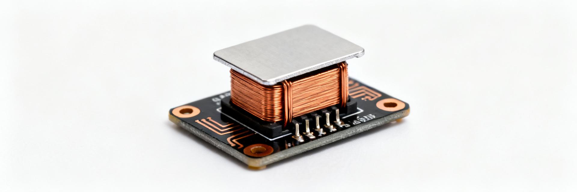
AMELH5030S-1R8MT: Full Electrical Specs & Footprint
Key Takeaways
- Space Efficiency: The 5x3mm footprint reduces PCB area by ~25% compared to standard 6x6mm inductors.
- High-Load Stability: 6A saturation current supports high-peak rails without inductive collapse.
- Thermal Optimization: Low 28mΩ DCR minimizes heat dissipation, extending component lifespan in tight enclosures.
- EMI Shielding: Molded construction provides superior magnetic shielding for noise-sensitive analog circuits.
In modern compact DC–DC converters, a single‑µH change in inductance or a milliohm of extra DCR can shift efficiency by tenths of a percent and force thermal redesigns. This guide compiles the definitive electrical specs and PCB footprint guidance for the AMELH5030S-1R8MT so designers can make accurate BOM and layout decisions, reduce iteration cycles, and avoid late-stage board rework.
Background: What the AMELH5030S-1R8MT is and typical use cases
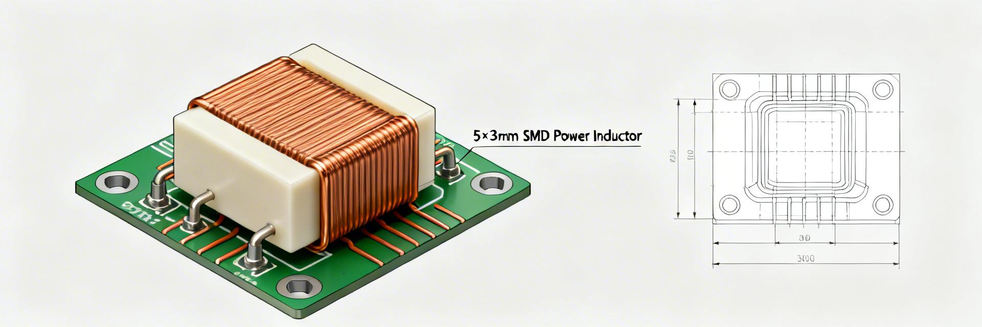
Market Comparison: AMELH5030S-1R8MT vs. Generic Power Inductors
| Feature | AMELH5030S-1R8MT | Standard 5030 Inductor | Design Impact |
|---|---|---|---|
| Saturation Curve | Soft Saturation (Molded) | Hard Saturation (Ferrite) | Prevents sudden peak current trips |
| EMI Shielding | Full Internal Shielding | Partial/External | Simplifies FCC/CE compliance |
| DCR Tolerance | Tight (±10% Range) | Wide (±20%+) | Predictable thermal modeling |
Mechanical summary & package outline
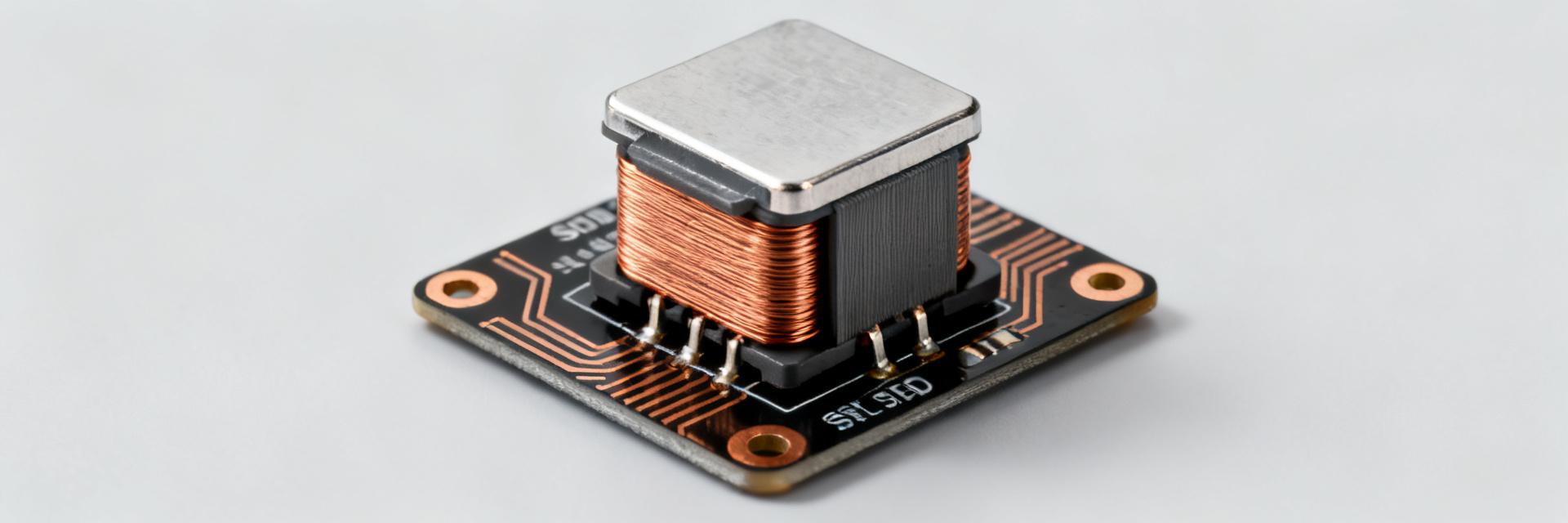
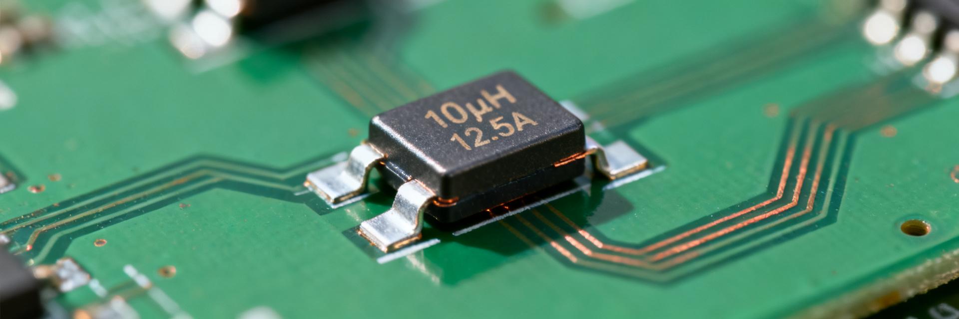
Point: The AMELH5030S-1R8MT is an SMD molded/shielded power inductor in a 5.0×3.0 mm nominal envelope frequently selected for space‑constrained power stages. Evidence: Package drawings list the part family as a low‑profile, rectangular molded package with defined land pattern references. Explanation: For PCB land‑pattern decisions extract the L×W×H dimensions from the datasheet, then apply the manufacturer pad span and recommended pad fillet to ensure consistent solder fillets and pick‑and‑place accuracy.
- L×W×H (typical): 5.0 × 3.0 × 1.8 mm — Saves vertical clearance in mobile designs.
- Package type: SMD molded, shielded — Reduces crosstalk between switching nodes.
- Typical weight: ~10–20 mg — Suitable for high-vibration applications.
- Footprint callouts: reference land pattern span, pad lengths, and recommended solder mask openings.
Typical electrical role & application scenarios
Point: A 1.8 µH SMD inductor like this is commonly used in synchronous buck converters and post‑regulator LC filters where compactness and moderate current capability are needed. Evidence: Typical application notes position 1.8 µH parts in 1–5 A output rails at switching frequencies from a few hundred kHz up to several MHz. Explanation: Choose this part when the expected ripple current and DC bias keep inductance within your designed margin; consider higher inductance for lower switching frequency or higher ripple filtering, and lower inductance for higher switching frequencies and smaller ripple current.
"When integrating the AMELH5030S-1R8MT, many engineers overlook the Saturation Margin. At 1.8µH, this part is optimized for 1-2MHz switching. However, if your peak current exceeds 5.5A, the inductance drop can cause the controller to trigger over-current protection. I recommend keeping the continuous DC load at 4.5A and reserving the rest for transient spikes. Also, ensure your ground plane 'keep-out' directly under the inductor is respected to minimize parasitic capacitance."
Electrical specs deep-dive
Key declared specs to list with units and tolerances
| Spec name | Symbol | Typical | Max | Units | Notes |
|---|---|---|---|---|---|
| Nominal inductance | L | 1.8 | ±20% | µH | Measured at 100 kHz, 0.1 Vrms |
| DC resistance | DCR | 28 | 50 | mΩ | Typical/max at 25°C |
| Rated current (saturation) | Isat | 6 | — | A | ΔL ≤ 30% criterion |
| RMS current | Irms | 4.5 | — | A | Thermal rise limit |
Footprint & PCB layout recommendations
Hand-drawn schematic, not a precise circuit diagram.
Point: A CAD‑friendly land pattern block reduces soldering defects and alignment issues. Evidence: Datasheet footprint drawings provide pad geometry (pad length, width, spacing) and recommended solder mask clearances. Explanation: Implement pad dimensions with ±0.05 mm tolerances in the CAD library, use a 60–80% paste aperture for each pad to control solder volume, and keep solder mask openings consistent with manufacturer guidance to avoid tombstoning.
- Pad geometry: pad length 3.0 ±0.05 mm, pad width 1.2 ±0.05 mm.
- Solder mask: 0.15 mm clearance beyond pad edges for stable wetting.
- Paste stencil: 0.12–0.15 mm thickness; 60–80% aperture coverage.
Testing, validation & reflow profile
Point: Prototype validation should confirm datasheet claims under realistic conditions. Evidence: Typical prototype tests include DCR, inductance at DC bias, impedance sweep (L and Q), SRF identification, and thermal rise under rated current. Explanation: Use a calibrated LCR meter for inductance at specified frequencies; accept deviations within datasheet tolerances and log any thermal rise beyond specified Irms limits.
Troubleshooting Checklist
- Excessive Heat? Check if DC load exceeds 4.5A or if nearby components are heating the inductor.
- Audible Noise? Verify switching frequency is outside the human audible range (20Hz-20kHz) and ensure the part is securely soldered.
- Inductance Drop? Measure current with a probe to see if peak transients are hitting the saturation point (6A).
Summary
This guide distilled critical electrical specs and PCB footprint guidance for the AMELH5030S-1R8MT to help power designers finalize BOM and layout with confidence. Key takeaways: verify DC‑bias curves and DCR against expected operating current, follow the recommended land pattern and paste guidance, and validate with prototype tests and reflow checks before production.
Frequently asked questions
How should I verify the inductance vs current behavior?
Measure L with an LCR meter while applying a controlled DC bias current. Ensure inductance stays within design margin at peak current.
What solder stencil aperture works best for this package?
A 60–80% area aperture per pad with 0.12–0.15 mm thickness reduces tombstoning and ensures reliable fillets.