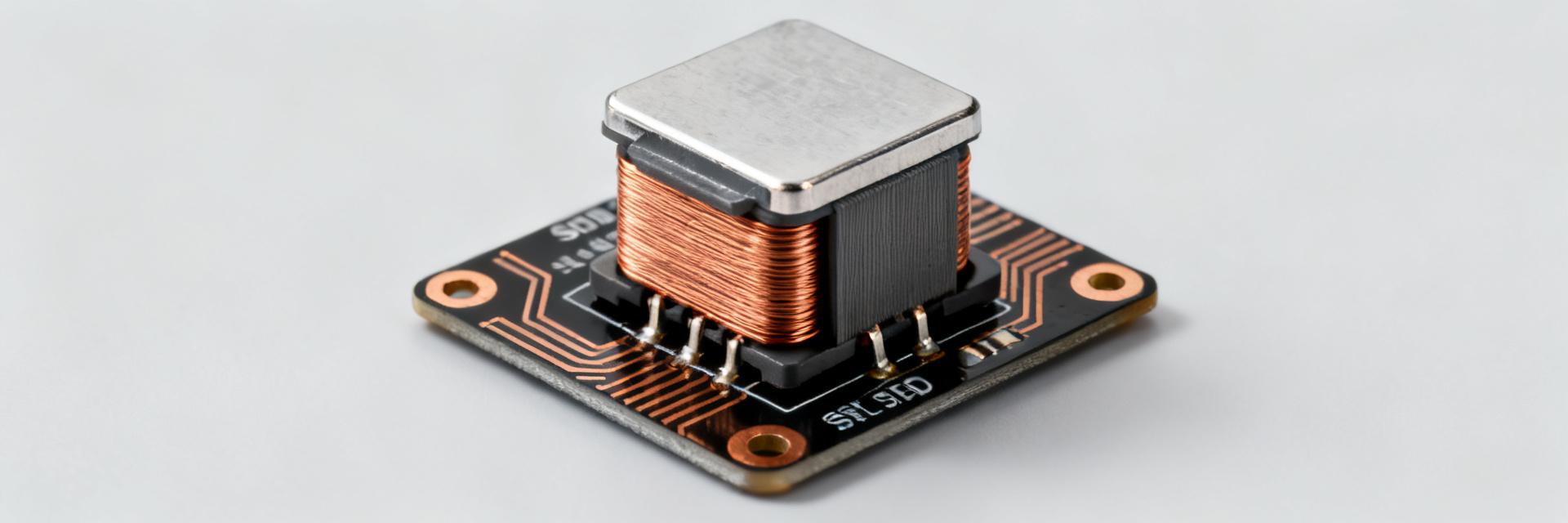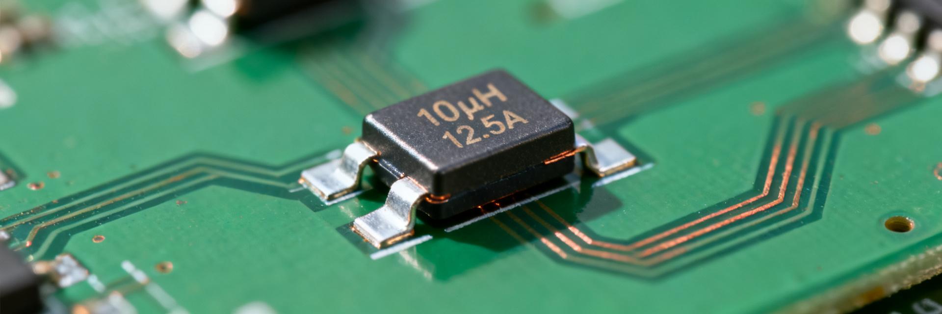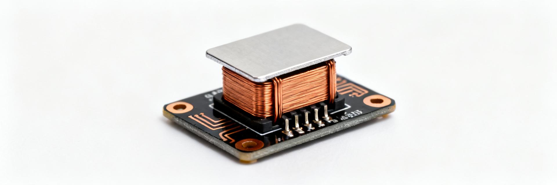
Point: Power SMD inductors in the high-current, low-inductance class typically cover nominal inductances in the microhenry to single-digit microhenry range with rated currents from several amps up to tens of amps. Evidence: In practice, engineers expect low DCR (single-digit milliohms), saturation behavior that reduces L significantly under DC bias, and measurable thermal rise when operated near Irms. Explanation: Accurate Specs and Ratings matter because inductance under DC bias, DCR, and thermal performance directly affect converter ripple, efficiency, and reliability during prototyping and production.
Point: This article is an actionable reference that consolidates specifications, interprets ratings, and outlines step-by-step test procedures. Evidence: It targets bench validation for PCB-mounted power modules and buck converters where inductor behavior under DC bias and thermal stress is decisive. Explanation: The guide names the part HPAL1V0650-1R0-R once and walks engineers through what to verify on the datasheet, how to test on-board and off-board, and how to interpret failures so designs meet performance and reliability goals.
Product snapshot — what HPAL1V0650-1R0-R is and where it fits (Background)
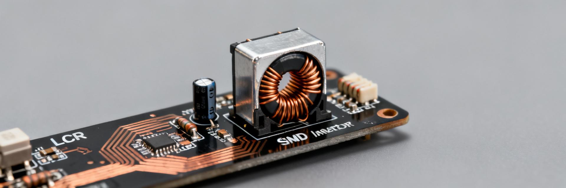
Key identity & quick specs
Point: At a glance, this SMD 2-pad power inductor is intended for point-of-load converters and high-current buck applications. Evidence: Confirm the exact nominal inductance, rated current, package style and common use-cases against the component datasheet. Explanation: Below is a compact, fillable table for rapid verification during procurement or design review.
| Field | Value (fill from datasheet) |
|---|---|
| Part number | HPAL1V0650-1R0-R |
| Inductance | 1.0 μH (nominal) |
| Tolerance | ±20% (typical) |
| Rated current (Irms) | — A (Refer to target thermal delta-T) |
| Saturation current (Isat) | — A (defined drop %) |
| DCR | — mΩ @ 25°C |
| Height / Pads | — mm / SMD 2-pad |
Typical use-cases & performance expectations
Point: In real circuits, expect the inductor to trade size and DCR against current handling and SRF. Evidence: Designers normally target inductance within ±10% under specified DC bias and accept modest efficiency losses if DCR is higher. Explanation: Recommended test targets include L within ±10% of nominal at the datasheet test frequency with rated DC bias and DCR matching datasheet values at 25°C; thermal derating should be planned based on PCB copper and ambient conditions.
Complete electrical & mechanical specs (Data & Ratings deep-dive)
Electrical characteristics and ratings (Inductance, DCR, Isat, Irms, SRF)
Point: Key electrical parameters to capture are nominal inductance (with test frequency), DCR at 25°C, Irms, Isat (datasheet-defined % L drop), SRF and temperature coefficient. Evidence: Ratings are meaningful only with test conditions—frequency, excitation level, and temperature—listed on the datasheet. Explanation: When you record Ratings, note the measurement frequency for L, the definition used for Isat (commonly 10–30% L drop), and the DCR measurement method; this ensures bench results map to datasheet claims.
Mechanical, thermal & assembly specs (dimensions, reflow, solderability)
Point: Mechanical and thermal data determine assembly feasibility and thermal performance on-board. Evidence: Capture part dimensions, recommended pad footprint, maximum operating temperature, and the reflow profile (peak temp and time above liquidus) from the vendor documentation. Explanation: Also log packaging format (tape & reel), weight, and handling notes; these affect pick-and-place, hand-soldering risk, and thermal coupling to PCB copper pours used for heat spreading.
How to interpret ratings and choose the right inductor (Method / selection guidance)
Current ratings, derating and real-world limits
Point: Irms and Isat are different: Irms limits thermal rise during continuous operation, Isat defines core linearity under DC bias. Evidence: A practical derating rule of thumb is to use a safety margin on Irms based on ambient and PCB thermal resistance; many engineers pick 60–80% of Irms for continuous loads in moderate ambient. Explanation: Exceeding Isat causes L to collapse, increasing ripple and core loss; exceeding thermal limits degrades solder joints and accelerates aging, so both electrical and thermal derating must be applied.
Matching part to topology & switching frequency
Point: Inductance selection depends on switching frequency and allowable ripple current. Evidence: Higher switching frequencies allow smaller inductance but often increase switching losses and reduce SRF margin; lower DCR yields higher efficiency but usually larger package. Explanation: Balance these tradeoffs: choose inductance to keep ripple within design goals, confirm DCR impact on efficiency, and ensure SRF is well above switching frequency to avoid resonance issues. Long-tail keywords to target include selection guidance and derating rules.
Test guide — bench procedures, equipment & pass/fail criteria (Methods / Test Guide)
Bench tests: inductance, DCR, Q and SRF (step-by-step)
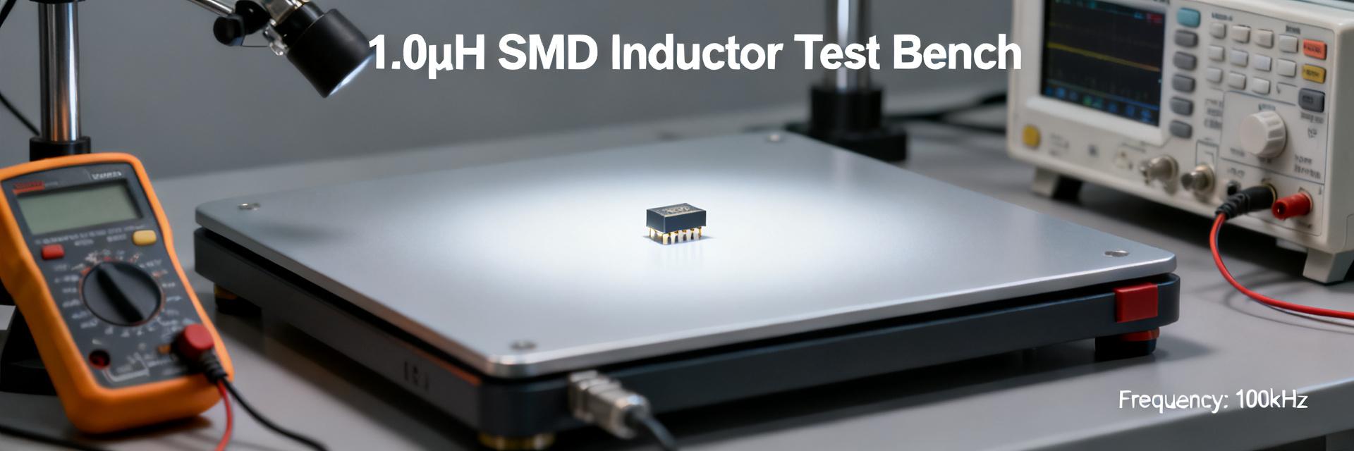
Point: A standard bench setup includes an LCR meter, impedance analyzer, four-wire DCR meter and an oscilloscope with current source. Evidence: Test steps: 1) Measure no-bias inductance at specified frequency and record; 2) Measure DCR with four-wire method at 25°C; 3) Sweep Q and SRF with impedance analyzer. Explanation: Acceptable tolerances should reference datasheet numbers; log test temperature, frequency, L, DCR, Q and setup notes in a table to ensure traceability.
Data logging template structure: test temp, test frequency, L (μH), DCR (mΩ), Q, SRF (MHz), measurement setup.
High-current / saturation & thermal tests (step-by-step)
Point: Saturation and thermal behavior are validated by controlled DC bias and board-mounted thermal testing. Evidence: Procedure: ramp DC through the inductor while measuring L; define Isat per datasheet (e.g., current at X% L drop); run steady-state Irms on a board while monitoring top-of-part temperature with a thermocouple for a set duration. Explanation: Define pass/fail thresholds (L within spec at bias, thermal rise below specified ΔT); use current limiting and thermocouples for safety and correlate failure modes—excess heating, L degradation, or solder joint failure.
- Prepare board-mounted sample with representative copper pour and thermal vias.
- Measure baseline L and DCR at 25°C.
- Ramp DC to Isat definition point, record L vs. I curve.
- Apply rated Irms for designated time, log temperature rise.
- Assess pass/fail against datasheet Ratings and thermal limits.
Application notes, PCB layout, reliability & troubleshooting (Case study + action)
PCB layout & thermal management best practices
Point: Layout directly affects thermal dissipation and EMI. Evidence: Use short current loops, optimized pad geometry, thermal vias under or beside the inductor, and a solid copper pour connected to the return to spread heat. Explanation: Also ensure mechanical stress relief, keep high-current traces short, and respect pick-and-place tolerances to avoid tombstoning or misalignment during reflow.
Common failure modes and practical fixes / buying checklist
Point: Typical issues include unexpected saturation under DC bias, excessive heating due to ripple, solder defects, and incorrect footprint selection. Evidence: A concise pre-purchase checklist: confirm inductance at bias, DCR @ 25°C, Isat definition, Irms rating, package dimensions, reflow profile and sample test reports. Explanation: Request sample parts and run the outlined tests on representative boards before production to avoid field failures. Recommended long-tail searches include test procedure and PCB layout tips.
Key summary
- HPAL1V0650-1R0-R fits high-current point-of-load roles; verify inductance, DCR and Irms from the datasheet before layout and procurement.
- Confirm Ratings definitions—Isat drop %, DCR test conditions, and Irms thermal limits—so bench results match vendor claims and design margins.
- Follow the step-by-step bench and thermal tests: baseline L/DCR, L vs. DC bias, and steady-state thermal rise on-board with thermocouple monitoring.
- Apply PCB layout best practices: short loops, thermal vias, copper pour for heat spreading, and correct footprint to reduce soldering issues.
FAQ
How do I verify HPAL1V0650-1R0-R inductance under DC bias?
Measure baseline inductance with an LCR meter at the datasheet test frequency, then ramp DC current while recording L using an impedance analyzer or suitable LCR meter with bias capability. Define Isat using the datasheet's specified percent L drop—record the L vs. I curve to validate compliance.
What acceptance criteria should I use for HPAL1V0650-1R0-R thermal ratings?
Use the datasheet Irms rating and measure temperature rise during a steady-state test on a representative PCB. A typical pass criterion is that top-of-part temperature rise stays below the vendor-stated ΔT or conservative limits (e.g., <40–60°C rise) depending on solder and board materials—always reference the datasheet Ratings when available.
Which tests confirm DCR and solder joint reliability for HPAL1V0650-1R0-R?
Confirm DCR with a four-wire measurement at 25°C and after thermal soak to detect drift. For solder reliability, run reflow with the specified profile, perform visual inspection, and cycler thermomechanical stress tests if production volumes warrant—identify cracks, tombstoning, or joint fatigue early.
How do I optimize the PCB layout for HPAL1V0650-1R0-R electromagnetic compatibility?
Keep current loops as short and wide as possible, routing the switching node away from sensitive analog circuits. Place a solid ground plane directly beneath the inductor component layer to shield capacitive switching noise, and keep the inductor pad spacing identical to the datasheet recommendations to eliminate tombstoning risk.