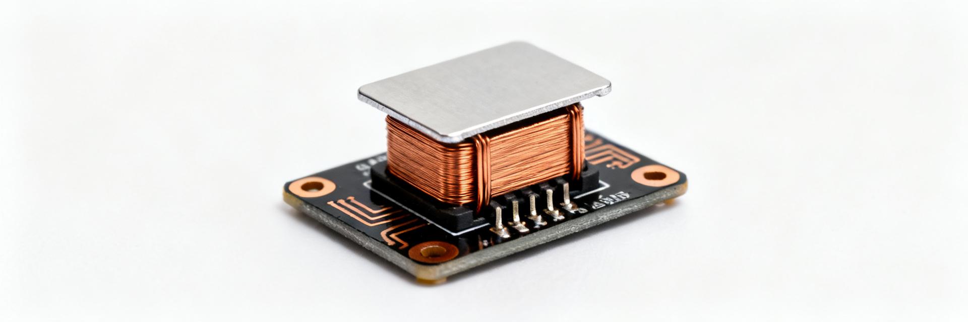
AMELH6020S-1R8MT SMD Inductor: Detailed Specs & Test
The AMELH6020S-1R8MT is documented in vendor datasheets as a 1.8 μH SMD inductor in a 6.8 × 6.6 × 2.1 mm molded package with industry-grade current and saturation specifications. This fact sets expectations for engineers selecting compact power inductors for switching regulators and EMI filters: you get a moderate inductance in a tightly packaged form factor designed for surface-mount assembly and power applications. This article’s goal is to provide a compact, testable, SEO-ready reference of AMELH6020S-1R8MT specs, reproducible measurement procedures, and practical pass/fail criteria for PCB qualification. It summarizes the electrical and mechanical headline values, explains how SRF and DCR affect real-world performance, prescribes benchtop validation steps including fixture compensation and thermal monitoring, and offers actionable purchase and in-lab qualification checklists so a design engineer can move from datasheet to validated board-level use with confidence.
1 — Product Overview & Key Specs (background)
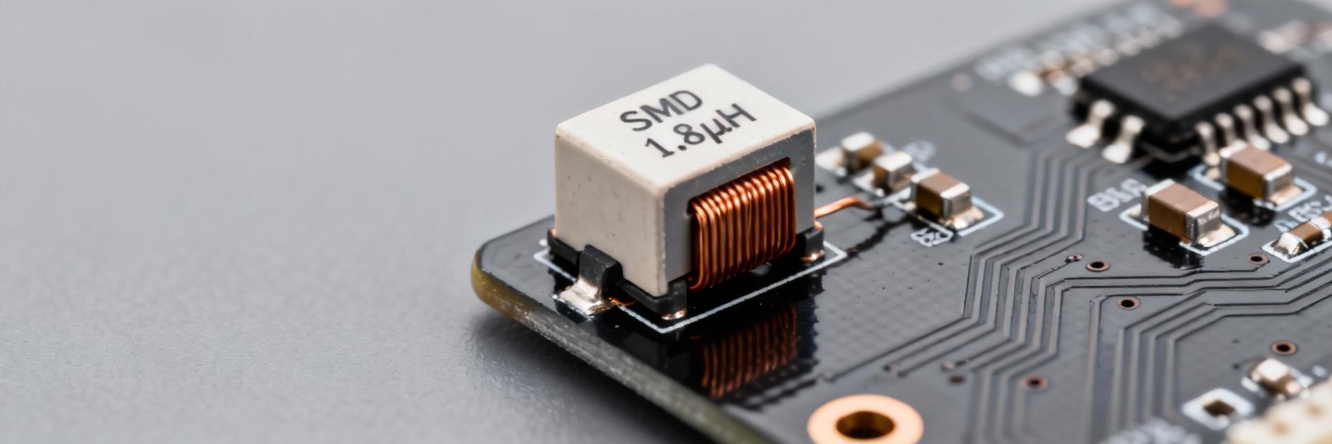
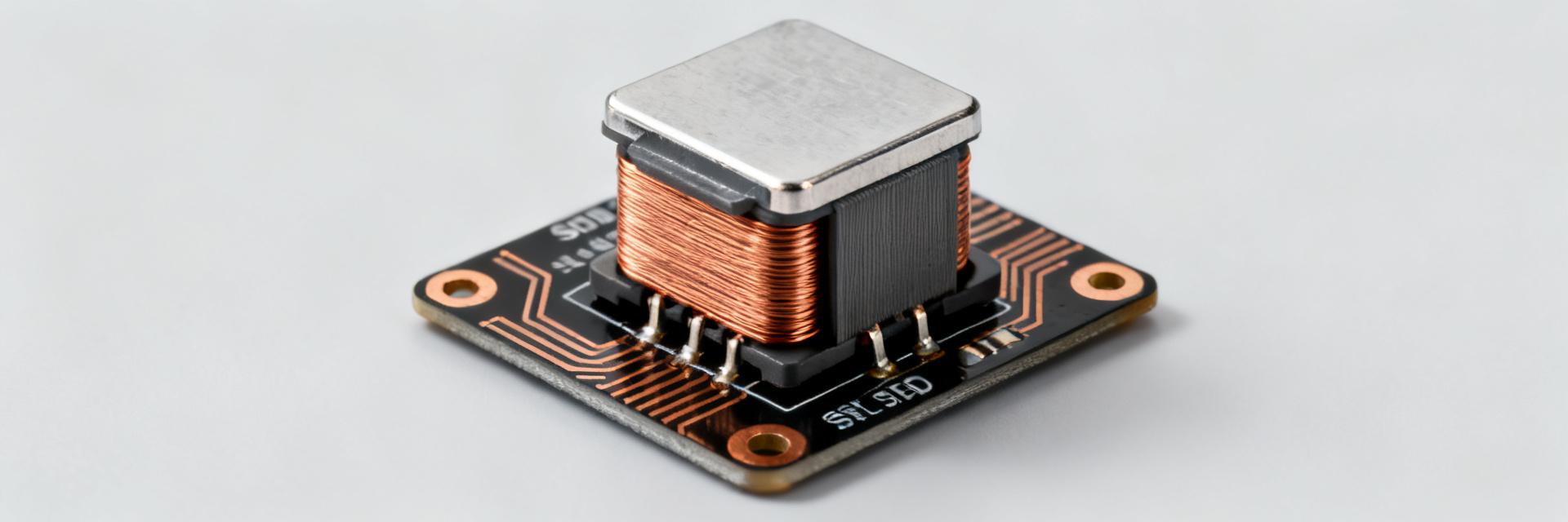
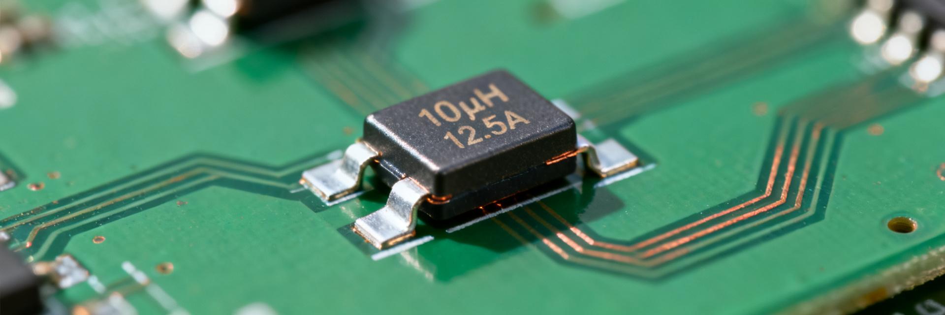
This section consolidates the headline specs engineers need to compare and qualify the AMELH6020S-1R8MT SMD inductor against design targets. The part is a molded power inductor with an inductance of 1.8 μH and typical power-focused attributes: low DC resistance for efficiency, a rated current and a saturation current that define usable ripple margins, and a self-resonant frequency (SRF) that bounds high-frequency behavior. The footprint is 6.8 × 6.6 × 2.1 mm with flat terminals for standard reflow mounting. Use these condensed specs as the first filter when creating a BOM entry or a component shortlist for buck converters or input filters.
1.1 — Official datasheet snapshot (what to list)
Key headline items to extract from the AMELH6020S-1R8MT datasheet specs are: inductance = 1.8 μH (stated tolerance), DC resistance (DCR) typical and maximum, rated current (thermal rating for acceptable temperature rise), saturation current (ISAT defined as % drop in inductance at DC bias), self-resonant frequency (SRF), mounting/termination type (SMD molded flat-plate terminations), package size 6.8 × 6.6 × 2.1 mm, and operating temperature range. Also capture recommended pad geometry and reflow profile notes. Record manufacturer part number variants and packaging code to ensure correct reel/box ordering and traceability on the BOM.
1.2 — Electrical and mechanical parameters explained
Define each spec for decision-making: DCR impacts conduction loss (Pcond = I^2 × DCR), so lower DCR improves converter efficiency but often increases size or cost; SRF is the frequency where inductive behavior turns capacitive and should exceed the converter’s switching harmonics to avoid attenuation or resonance issues; saturation current denotes the DC bias level at which inductance drops (commonly specified at a defined % drop such as 30%); thermal rating and rated current combine to define acceptable continuous currents with limited temperature rise. Typical vendor ranges for similar molded parts: DCR from single-digit milliohms up to a few hundred milliohms depending on inductance and current rating; SRF often lies in the 100–300 MHz region for compact power inductors, but verify on the specific datasheet for AMELH6020S-1R8MT.
1.3 — Packaging, footprint and BOM considerations
Recommended pad geometry should follow the manufacturer’s land pattern to minimize tombstoning and ensure reliable solder fillet formation; use the datasheet’s pad layout and stencil aperture guidelines. Follow standard Pb‑free reflow profiles with controlled peak temperature and soak sufficient for the molded body. Handle as ESD-sensitive when appropriate and accept standard storage shelf-life and moisture-sensitivity levels per packaging notes. For procurement, capture manufacturer, full part number (including tolerance suffixes), reel size, and country of origin on the BOM; note minimum order quantities and lead times to avoid schedule slips in production.
2 — Performance Data & When It Matters (data analysis)
Understanding where the AMELH6020S-1R8MT’s electrical behavior interacts with your circuit is essential. Frequency response, DCR, and current handling each dominate different failure or performance modes: SRF limits the upper usable frequency, DCR controls steady-state conduction losses, and saturation/thermal limits dictate safe ripple and DC bias choices. This section shows how to interpret vendor curves and translate them into design margins, derating, and acceptance criteria for PCB use.
2.1 — Frequency response and SRF implications
For similar molded power inductors SRF typically falls in the 100–200 MHz range; above SRF the part becomes capacitive and fails to act as an inductor at those harmonics. Engineers should request or measure L vs. frequency to plot inductance decay, with a logarithmic frequency axis to visualize the usable band. Expected curve shapes: relatively flat L in the low kHz to low MHz, then a gradual roll-off as parasitic capacitance appears, culminating in SRF where |Z| peaks. For switching regulators running dozens to low hundreds of kHz, the SRF is usually not a limiting factor, but for converters with high harmonic content or radio-frequency front-ends, verify the AMELH6020S-1R8MT frequency response before acceptance.
2.2 — DC resistance (DCR) vs. efficiency trade-offs
DCR directly translates to conduction losses: P_loss = I_rms^2 × DCR. For example, with a DCR of 50 mΩ a 1 A RMS current dissipates 50 mW, while 2 A RMS dissipates 200 mW; these losses translate to reduced converter efficiency and local heating. Create a simple table during selection with columns: operating current, I^2×DCR loss, and estimated temperature rise (use thermal characterization or vendor thermal impedance). When selecting AMELH6020S-1R8MT for efficiency-sensitive designs, compare its DCR to lower-DCR alternatives and consider trade-offs with size and SRF.
2.3 — Current handling: rated, saturation, and thermal limits
Rated current is typically defined by an allowable temperature rise (e.g., ΔT = 40 °C) and represents a continuous current the part can handle thermally. Saturation current specifies the DC bias at which inductance falls by a specified percentage (often 20–30%). Choose the inductor so that the expected peak and RMS currents, including ripple, stay below both thermal and saturation limits; a practical derating is 20–30% margin on rated current for continuous operation to preserve life and linearity under transients.
3 — Test Procedures: How to Validate AMELH6020S-1R8MT on Benchtop (methods guide)
To move from datasheet to qualified component on the PCB, perform benchtop validation that measures the same parameters the datasheet reports and simulates real operating stress. This section lists equipment, step-by-step electrical test procedures with fixture compensation, and thermal/real-world load tests to detect early failures.
3.1 — Required equipment and calibration
Essential instruments: an LCR meter (1 kHz–1 MHz) for baseline inductance and DCR, an impedance analyzer or VNA (to 100+ MHz) for SRF and L vs. frequency sweeps, a calibrated DC current source for saturation testing, a thermal camera or thermocouples for temperature rise measurement, and low-parasitic test fixtures or PCBs with Kelvin pads. Calibrate instruments per manufacturer instructions and perform open/short compensation on fixtures to remove parasitic inductance and capacitance; document compensation files and background noise floor before collecting component data.
3.2 — Step-by-step electrical tests
Reproducible test sequence: 1) Measure DCR using a four-wire method at ambient temperature. 2) Measure L at multiple frequencies (1 kHz, 10 kHz, 100 kHz, 1 MHz) on the LCR meter to capture inductance drift. 3) Perform an impedance sweep with the impedance analyzer to locate SRF (observe magnitude and phase peaks). 4) Measure inductance vs. DC bias by incrementally applying DC current and recording L at each bias point to determine saturation current where L drops by the datasheet’s % threshold. Use test levels and pass/fail thresholds set to datasheet tolerances (e.g., ±20% inductance tolerance) and log all instrument settings for traceability.
3.3 — Thermal and real-world load testing
Run a steady-state load test on a representative PCB section: apply the expected DC plus switching ripple waveform (or an equivalent DC bias with a superimposed AC ripple) and monitor case and nearby PCB temperatures with a thermal camera and thermocouples at defined monitoring points. Recommended duration is sufficient to reach steady temperature—typically 30–60 minutes—under worst-case ambient. Red flags include temperature rise above the rated ΔT limit, continuous inductance drift under bias, unexpected SRF shifts, or visible damage such as cracking or delamination after reflow and thermal cycling.
4 — Comparative Cases & Application Notes (case study)
Use-case examples illuminate how the AMELH6020S-1R8MT SMD inductor performs in practice and how alternatives change design trade-offs. Below we present a typical buck converter selection exercise, a compact comparison table versus nearby alternatives, and observed field failure modes with mitigation strategies.
4.1 — Typical application: buck regulator example
For a synchronous buck at 500 kHz targeting 2 A load with 30% peak-to-peak ripple current, choose an inductance that yields acceptable ripple (ΔI = Vout × (1−D) / (L × Fs)); with 1.8 μH the expected ripple at 500 kHz can be calculated and compared to allowed inductor ripple. The AMELH6020S-1R8MT’s DCR and rated current determine conduction loss and thermal margin; place the inductor close to the switching node with a short return path, maintain solid copper under the component for heat conduction, and follow recommended pad geometry to reduce solder-related reliability issues.
4.2 — Comparison vs. similar parts (size/performance trade-offs)
| Part | Inductance | DCR (typ) | Rated Current | SRF (typ) |
|---|---|---|---|---|
| AMELH6020S-1R8MT | 1.8 μH | (vendor spec) | (vendor spec) | (vendor spec) |
| AMELH6020S-1R5MT | 1.5 μH | lower/higher depending | similar | similar |
| Alternative 4.7 μH (same footprint) | 4.7 μH | higher | lower | lower |
Pros/cons: choose AMELH6020S-1R8MT when footprint and current rating align with efficiency needs; consider lower-DCR alternatives if efficiency is paramount, or higher-inductance parts if ripple must be minimized at the expense of DCR or SRF.
4.3 — Failure modes observed in field/test
Common failures include saturation when ripple or DC bias exceeds design limits, solder fillet cracking from inadequate pad design, and thermal degradation from insufficient derating. Diagnose failures by repeating L vs. DC bias and thermal tests, inspecting solder joints microscopically, and correlating field waveforms to benchtop stress tests. Mitigations: increase margin on rated current, improve thermal conduction on PCB, adjust pad geometry per datasheet, and add heat spreading copper where feasible.
5 — Practical Checklist & Purchase/Qualification Steps (action recommendations)
Before placing the AMELH6020S-1R8MT on a PCB, follow a structured procurement and qualification workflow: cross-check datasheet specs against design requirements, verify supplier traceability and RoHS/compliance claims, ensure packaging and reel formats match assembly equipment, and plan a minimal in-lab qualification sequence to confirm DCR, L@f, SRF spot-check, reflow survivability, and thermal performance under expected currents.
5.1 — Pre-purchase checklist for engineers
Verify: (1) Inductance and tolerance meet the design margin; (2) DCR consistent with efficiency targets; (3) rated and saturation currents exceed expected DC plus ripple currents with 20–30% derating; (4) manufacturer and distributor traceability; (5) RoHS and material compliance; (6) packaging codes and MOQ and lead time acceptable for project schedule.
5.2 — In-lab qualification checklist
Minimum test battery before PCB approval: measure L at working frequency and at 1 kHz baseline, measure DCR (4-wire), sweep impedance to confirm SRF, perform L vs. DC bias to find saturation behavior, thermally load at expected current for steady-state ΔT assessment, and run a reflow survivability test with post-reflow electrical checks. Recommended sample size for incoming QA: a statistically justifiable lot sample (e.g., 9 per reel for initial qualification) and periodic sampling in production.
5.3 — Documentation & reporting template (what to include)
Test report should include: summary verdict, component identifiers, test conditions (temperature, fixture, instrument models), raw data files, plots (L vs. f, impedance magnitude/phase, L vs. DC bias), thermal images and thermocouple logs, photographs of solder joints, pass/fail criteria with disposition, and recommended mitigation if marginal. Preserve data for supplier discussions and change control.
Summary
The AMELH6020S-1R8MT is a compact 1.8 μH SMD inductor packaged at 6.8 × 6.6 × 2.1 mm whose primary selection drivers are inductance, DCR, SRF, and current ratings. Engineers should validate the part on the bench with DCR, L@multiple frequencies, SRF sweeps, and L vs. DC bias to confirm saturation behavior, then perform thermal steady-state testing on the target PCB. For reliable operation, derate rated current by 20–30% for continuous use, follow manufacturer pad and reflow guidance, and document qualification results in a structured report. Next steps: apply the described tests, use the pre-purchase and in-lab checklists, and if margins are tight consider alternative parts with lower DCR or higher SRF as appropriate. This summary integrates the AMELH6020S-1R8MT SMD inductor specs into practical qualification steps for US-focused engineering teams.
Key Summary
- The AMELH6020S-1R8MT is a 1.8 μH SMD inductor in a 6.8×6.6×2.1 mm package; verify inductance and tolerance against design requirements before buying.
- Measure DCR and calculate I²·R losses at expected RMS currents to estimate efficiency impact and temperature rise on the PCB.
- Confirm SRF and L vs. frequency with an impedance analyzer to ensure inductive behavior across switching harmonics.
- Perform L vs. DC bias and thermal steady-state tests with derating (20–30%) as a practical pass/fail rule for continuous operation.
FAQ
What are the critical AMELH6020S-1R8MT specs I should verify before PCB placement?
Before placing the AMELH6020S-1R8MT on a PCB, verify inductance value and tolerance, DC resistance (DCR), rated current and saturation current specifications, and the self-resonant frequency (SRF). Also confirm package footprint, recommended land pattern, and reflow profile on the datasheet. Cross-check these against your converter’s switching frequency, expected ripple current, and thermal budget; any mismatch in SRF or insufficient current margin should prompt evaluation of alternative parts or layout changes.
How do I test AMELH6020S-1R8MT saturation and what pass/fail criteria should I use?
Measure inductance at a baseline frequency while incrementally applying DC bias current. Record the DC current where inductance falls by the datasheet’s specified percentage (often 20–30%); this is the saturation current. Pass/fail: the device should maintain required inductance within tolerance at the highest expected DC bias plus ripple; if the inductance drops below acceptable levels or the saturation current is below your worst-case peak, the part fails for that application and requires a higher-saturation alternative or redesigned ripple target.
What thermal test duration and monitoring points are recommended for AMELH6020S-1R8MT validation?
Run a steady-state thermal test long enough to reach equilibrium—typically 30–60 minutes—at the expected maximum operating current including ripple. Monitor the inductor case temperature and adjacent PCB temperatures with thermocouples or a thermal camera at defined points: top center of the component, terminal solder joints, and the nearest ground copper pour. Use the vendor’s ΔT-rated current as a guide: if measured ΔT exceeds the rated rise under test conditions, the component fails for continuous operation unless thermal mitigation is applied.