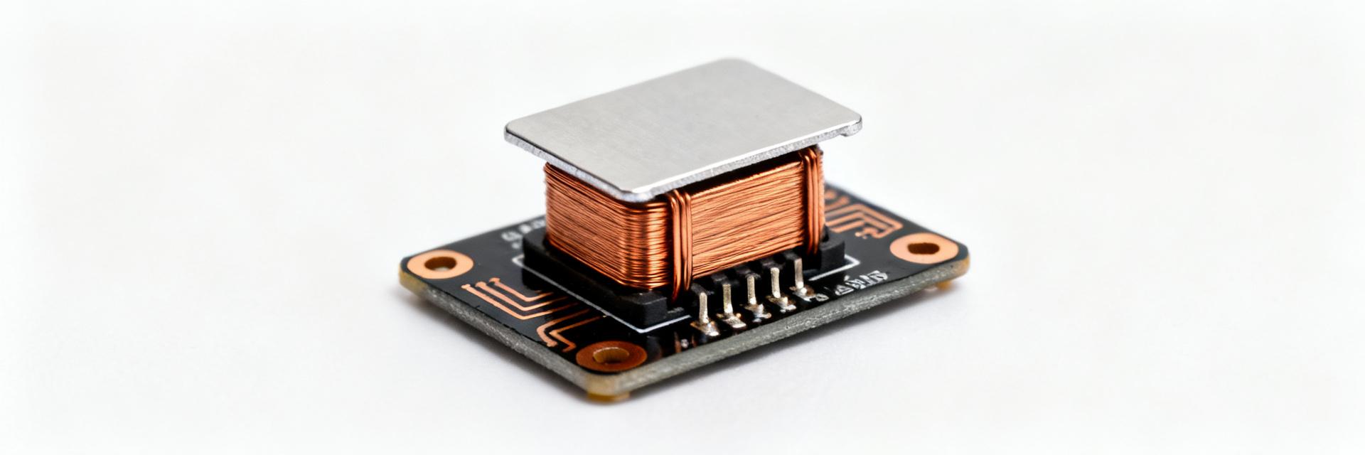
AMELH6060S-1R5MT Layout Metrics to Improve Power Supply
Careful, measurement-driven PCB work routinely shows that targeted layout changes materially reduce output ripple, EMI, thermal hotspots and IR-drop for power modules. Bench audits comparing baseline and optimized boards demonstrate measurable improvements when designers track concrete layout metrics. This article gives you specific metrics and validation steps to improve AMELH6060S-1R5MT performance using practical tests and clear targets.
This guide is written for PCB designers, power-electronics and test engineers focused on power supply layout. It outlines which metrics to track, how to measure them (scope setup, near-field and thermal scans), what baseline vs optimized comparisons to run, and a validation checklist you can follow during layout and debug.
1 — Why Layout Matters for AMELH6060S-1R5MT (Background introduction)
1 — Electrical performance consequences (what to measure)
Point: PCB parasitics—trace resistance, via impedance, and plane impedance—directly alter regulation, transient response and output ripple. Evidence: lab comparisons show loop inductance in the tens of nH produces measurable overshoot and added mVp‑p ripple. Explanation: measure loop inductance (nH), DC voltage drop (mV), transient settling time (µs) and output ripple (mVp‑p) using a low‑inductance scope probe or differential probing at the output nodes.
2 — EMI and thermal impact (what to measure)
Point: Layout drives both radiated/conducted emissions and local heating. Evidence: near-field scans commonly correlate large switching loop areas with high dBµV peaks at switching harmonics; thermal imaging shows hotspots where copper is insufficient. Explanation: record radiated emissions (dBµV at target bands), conducted EMI, PCB surface ΔT (°C) and hottest component junction temp using near‑field probe sets, EMI receiver and thermal camera under representative load.
2 — Key Layout Metrics to Track (Data analysis)
1 — Ground & power plane impedance metrics
Point: Plane resistance and AC impedance set available current and return behavior. Evidence: Kelvin DC resistance and impedance vs frequency traces reveal plane resonance and voltage gradients. Explanation: capture DC resistance (mΩ), AC impedance over frequency (Ω), and current density (A/mm²) via Kelvin measurements and impedance simulation; set targets relative to AMELH6060S-1R5MT load so voltage drop stays within a few tens of mV at full current.
2 — Loop area, return-path and stray inductance metrics
Point: Loop area is the dominant contributor to stray inductance and EMI. Evidence: measured reductions in loop area (mm²) correspond to nH-level inductance drops and lower EMI harmonics. Explanation: quantify loop area (mm²), estimate inductance with simple L ≈ μ0·area/height heuristics, and set thresholds (for example keep critical power loop area under X mm² for a given switching node) to limit transient overshoot and emissions.
3 — Trace, Via and Copper Metrics to Optimize (Method guide)
1 — Trace width, thickness and spacing (what to specify)
Point: Trace geometry controls IR drop and heating. Evidence: doubling copper weight or trace width lowers trace R (mΩ/cm) and reduces temperature rise under the same current. Explanation: specify trace R (mΩ/cm), current capacity (A), and target voltage drop per path (mV). Document minimum width, copper weight (oz/ft²) and derating in the PCB spec to ensure acceptable IR drop at expected currents.
2 — Via count, placement and electrical/thermal via metrics
Point: Vias influence DC resistance, inductance and heat flow. Evidence: adding parallel vias reduces per‑via DC resistance and spreads current, lowering hotspot ΔT. Explanation: specify via DC resistance, estimate via inductance, and require via stitching for power/return planes. Define minimum via counts near high‑current pads and thermal vias per pad (e.g., N vias to meet thermal target) for reliable current sharing and heat transfer.
4 — Component Placement & Thermal Management Metrics (Method guide)
1 — Placement rules tied to measurable outcomes
Point: Component proximity directly changes loop area and transient response. Evidence: moving decoupling capacitors within 2–5 mm of VIN/VOUT pins often halves measured loop inductance and improves settling. Explanation: enforce cap distance and trace length targets (mm) for decouplers, locate sense resistors on solid returns, and separate noisy power nodes from sensitive analog nets to reduce loop area and improve transient performance.
2 — Thermal spreading and cooling metrics
Point: Copper pours and thermal vias determine steady‑state temperatures. Evidence: increasing top/bottom copper and adding thermal vias reduces θJA and lowers board surface ΔT per watt. Explanation: set measurable thermal goals—allowed ΔT above ambient, copper area per watt, thermal vias per pad and target θJA (°C/W)—and validate with thermal imaging and power cycling to characterize steady and transient heating.
5 — Layout Case Study: AMELH6060S-1R5MT Baseline vs Optimized (Case display)
1 — Baseline metrics to capture (measurement protocol)
Point: Capture a complete baseline to quantify improvement. Evidence: baseline sets include output ripple, efficiency, transient response, EMI spectrum, hottest board temp and loop impedance. Explanation: use representative test conditions (input voltage, output current steps), probe at VIN, VOUT, switching node and ground with low‑inductance probes, and record ripple (mVp‑p), transient settling (µs), and EMI signatures for comparison.
2 — Optimizations implemented and resulting metric changes
Point: Sequence optimizations and re-measure after each change to isolate effects. Evidence: common interventions—plane stitching, shortened traces, added vias, cap repositioning and expanded copper—show consistent reductions in ripple, EMI peaks and hotspot temps. Explanation: re-measure the same metrics after each tweak and present before/after tables and plots to show reduced ripple, lower EMI amplitudes and decreased board temperatures qualitatively and quantitatively.
6 — Practical Pre/Post-Layout Checklist & Validation Steps (Actionable checklist)
1 — Pre-layout checklist (specify metric targets)
Point: Define targets before routing to guide decisions. Evidence: teams that document loop area limits, plane impedance targets, trace widths, via counts and cap placements see fewer iterations. Explanation: create a layout requirements sheet listing numeric targets (loop area limit, max plane DC resistance, min trace width, min via count, cap distance) so you can verify the finished layout meets measurable goals.
2 — Post-layout verification and iterative debug (how to validate)
Point: Systematic verification finds remaining issues quickly. Evidence: a repeatable routine—DC resistance checks, transient step tests, EMI scans and thermal imaging—lets you prioritize fixes. Explanation: for each test record the metric, compare to target, and if out of spec iterate on layout (add vias, shorten traces, move caps) until metrics meet the documented targets.
Summary
Tracking concrete layout metrics turns subjective layout discussions into measurable improvements. Use the outlined plane, loop, trace and thermal metrics to set targets, measure baseline behavior, apply targeted layout fixes and re-validate to lower ripple, EMI and hotspots. For the AMELH6060S-1R5MT, document targets, run the tests listed, and iterate until metrics meet your design requirements.
- Define plane and trace targets: set DC resistance (mΩ), AC impedance curves and current density limits to limit IR drop and maintain regulation using clear layout metrics.
- Minimize loop area and stray inductance: measure loop area (mm²) and estimate nH to reduce transient overshoot and EMI in your power supply layout.
- Specify trace/via thermal metrics: document copper weight, trace width, and number of thermal vias per pad to achieve target θJA and control hotspot ΔT under load.
- Validate with measurement-driven steps: perform baseline captures, apply incremental layout changes, and present before/after tables for ripple, EMI and temperature improvements.
Common Questions (FAQ)
How should I probe output ripple for AMELH6060S-1R5MT to get accurate layout metrics?
Use a short ground spring or a low‑inductance probe tip and differential probing at the output terminals; keep ground lead length minimal. Capture ripple at nominal load and transient steps, record mVp‑p across the bandwidth of interest, and log probe configuration so results are repeatable and attributable to layout, not measurement artifact.
What trace width and copper weight targets should I set for power paths?
Select widths that keep trace DC resistance low enough to limit voltage drop to your target mV under max current; use copper weight (oz) to improve thermal capacity. Document minimum width, expected mΩ/cm and current capacity, and include derating margins so layout meets both electrical and thermal targets.
Which thermal metrics are most actionable during layout verification?
Measure steady‑state ΔT above ambient at the hottest board location and estimate θJA from power dissipation. Use thermal imaging under representative loads to locate hotspots, correlate temperatures to copper area and via counts, and iterate until ΔT and θJA meet your documented targets for reliable operation.