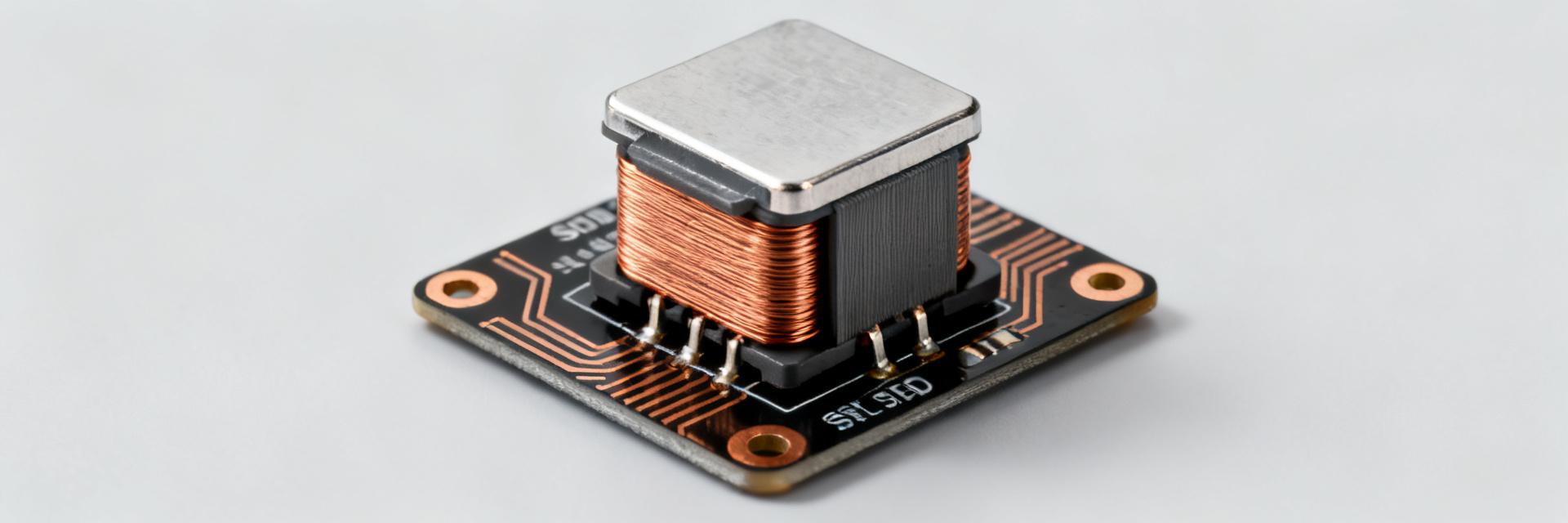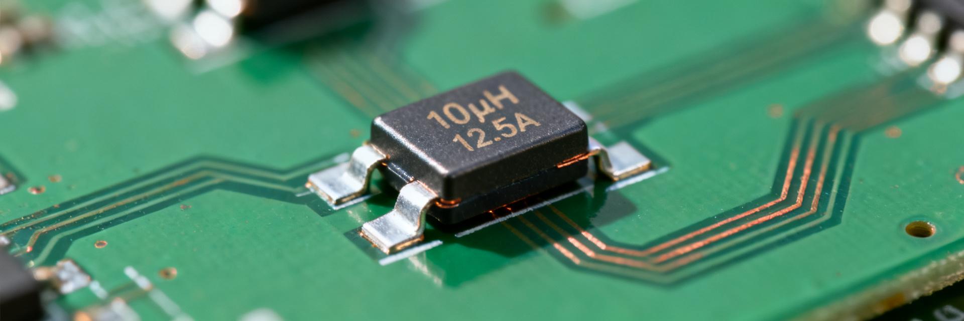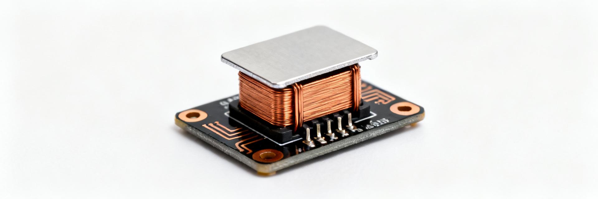
AMELH6020S-3R3MT: How to Read DCR, Isat & PCB Footprint
If you’re integrating the AMELH6020S-3R3MT into a power design, confusion around DCR, Isat and the correct PCB footprint slows development and risks field failures. This guide gives a step-by-step method to read those datasheet fields, convert numbers to real-world I²R losses and saturation margins, and produce a PCB land pattern that minimizes thermal and assembly risk.
All examples use unit-safe values and typical test conditions (25°C, kelvin measurement, and standard DC bias curves). Refer to the part datasheet tables for exact rows labeled inductance, DCR, Isat and mechanical drawing when you apply the checklist below.
Quick background: what AMELH6020S-3R3MT spec lines mean (background introduction)
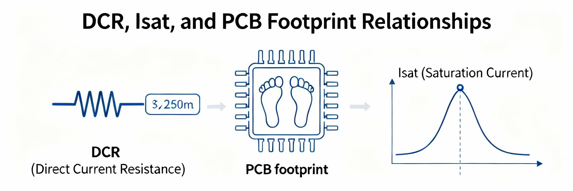
1.1 What the part designation and common table columns represent
Part numbers encode form factor and nominal inductance; the datasheet table lists columns for inductance (µH), tolerance (%), DCR (mΩ), Isat (A), test conditions and footprint drawing references. Look for test frequency and temperature notes—inductance is often measured at 100 kHz/0.1 Vrms and DCR at 25°C with a four-wire kelvin setup for accuracy.
1.2 Typical values and tolerances to expect for AMELH6020S-3R3MT
For this 3.3 µH class part expect DCR on the order of single- to low-double-digit milliohms and Isat ratings in the single to low‑double ampere range depending on core design. Tolerance (±%) shifts inductance and can change bias curves; manufacturer versus in-circuit measurements differ because nearby copper and DC bias alter apparent inductance and DCR.
How to read and use DCR (data analysis)
2.1 What DCR is, how it’s measured, and what the datasheet number means
DCR is the DC winding resistance in mΩ measured with a kelvin clamp at a stated temperature, usually 25°C. The datasheet value is a lab measurement; on-board DCR includes pad, via and trace resistance. Action: record the datasheet test conditions and verify with a bench kelvin measurement both off-board and soldered to capture assembly effects.
2.2 Using DCR to calculate I²R losses, temp rise, and efficiency impact
Use P = I²·R. Example: with DCR = 12 mΩ and DC current = 10 A, P = 10² × 0.012 = 1.2 W. Estimate temperature rise as P × thermal resistance; conservative thermal resistance for a small power inductor on a two-layer board may be 10–40°C/W depending on copper area, so expect 12–48°C rise. Translate loss to efficiency by dividing P by converter output power.
Interpreting Isat and saturation behavior (data analysis)
3.1 Isat definition, test conditions, and difference from rated/Irms
Isat is the DC current at which inductance drops by a specified percentage (often 10–30%) under stated test conditions. It is not a continuous thermal rating; Irms or current handling limits consider heating. Read the inductance vs DC bias curve in the datasheet to see how inductance degrades with DC current and use that to size headroom.
3.2 How to derate for transient currents, temperature, and margin calculations
Define peak expected current, compare to Isat and apply a safety margin (typical 30–50%). Example: if peak is 8 A and Isat = 12 A, a 33% margin exists; if you require 50% margin, choose a part with Isat ≥ 16 A or reduce ripple. Account for elevated temperature which shifts Isat downward and plan for transient headroom accordingly.
Reading the PCB footprint and land pattern (method / guide)
4.1 Decoding footprint drawings: pad sizes, tolerances, and keepouts
Transfer critical dimensions from the mechanical drawing to your CAD: pad length/width, pad pitch, component outline and solder mask openings in the same units shown. Create library pads using the recommended pad dimensions with fabricator tolerances; label reference planes and add a manufacturing note with units and datum to avoid misinterpretation of “mm” vs “inches.”
4.2 Assembly and thermal considerations: solder fillet, reflow, and via placement
Design pads to allow a reliable solder fillet and follow the recommended reflow profile in the datasheet. For heat dissipation, add thermal vias or copper pours tied to large planes; place vias outside the pad unless the datasheet explicitly supports via-in-pad. Include a small test pad or exposed trace for kelvin DCR checks after assembly.
Practical selection checklist + example design (case + action)
5.1 Step-by-step example: selecting AMELH6020S-3R3MT for a 3.3 V buck converter
Requirements: VIN 12 V, switching 500 kHz, max load 10 A, ripple target 20 mA. Use DCR to estimate conduction loss (example above), use Isat curve to ensure peak inductor current stays below Isat with 30–50% margin, then finalize footprint with recommended pad geometry and thermal copper to control temperature rise under worst case.
5.2 Pre-production verification checklist and measurement tips
Before production: (1) Kelvin DCR measurement off- and on-board, (2) inductance vs DC bias sweep to verify Isat behavior, (3) thermal imaging under load to confirm temperature rise, (4) solderability and fit checks. Acceptable deviations: DCR within +20% of datasheet and inductance degradation per bias curve within published tolerance.
Summary (conclusion)
- Read the datasheet rows for inductance, DCR and Isat and note test conditions to ensure valid comparisons to bench measurements of the AMELH6020S-3R3MT.
- Use P = I²·R with datasheet DCR and a conservative thermal resistance to size losses and estimate temperature rise for efficiency trade-offs.
- Pick Isat with 30–50% headroom against expected peaks and verify with inductance vs DC bias curves to avoid saturation-related regulation faults.
- Translate footprint dimensions precisely to CAD, add thermal copper or vias as needed, and keep measurement test pads for pre-production checks.
Frequently Asked Questions
How do I perform AMELH6020S-3R3MT DCR measurement on board?
Perform a four-wire kelvin measurement with the part soldered to its pads to capture assembly resistance. Use short test leads, record board copper geometry, and compare to off-board DCR. Expect on-board DCR to be higher by the trace+via resistance; allow up to +20% when qualifying the layout against the datasheet value.
How to read Isat values for design margining?
Read Isat as the current where inductance drops by a defined percent; then inspect the inductance vs DC bias curve. Select an Isat that gives 30–50% margin over expected peak current. For transient events, ensure the converter control can tolerate temporary inductance reduction without losing regulation.
What are the most common footprint mistakes that affect DCR and thermal performance?
Common mistakes: undersized pads that reduce solder fillet, lack of copper pour or thermal vias, and neglecting pad-to-plane connections. Each reduces heat spreading and raises temperature, which increases apparent DCR. Fix by following recommended pad sizes, adding copper area, and including test pads for post-reflow electrical checks.