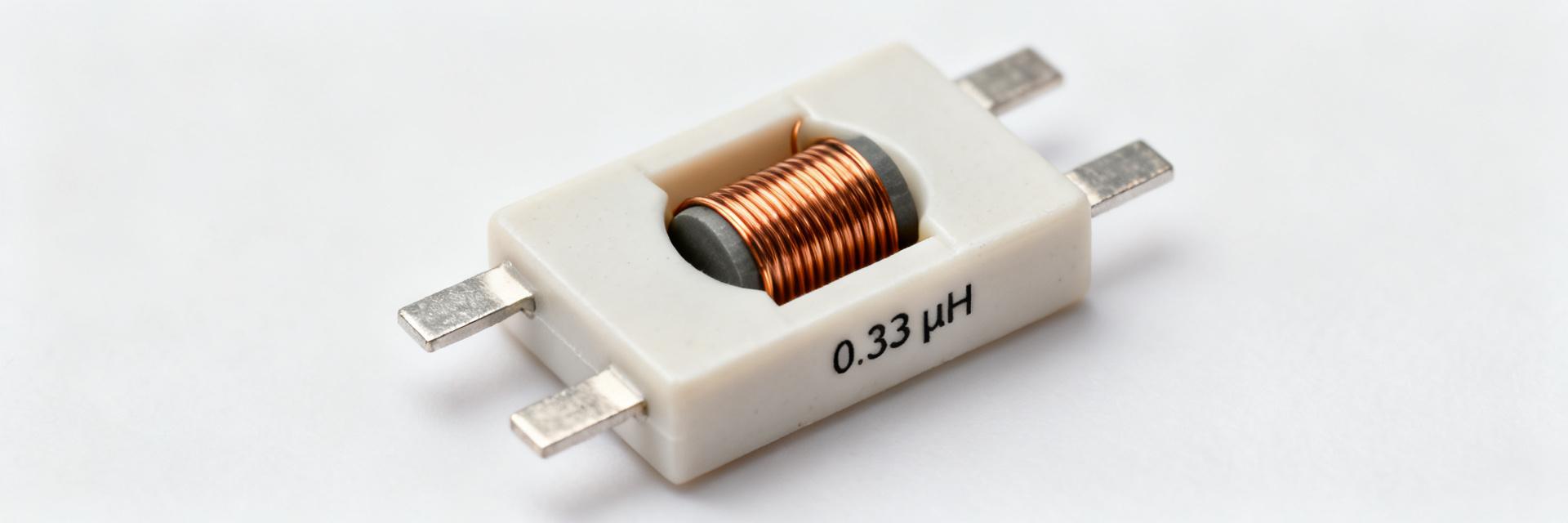
The HCM1A4020V3-R33-R is a high-performance, low-inductance surface-mount power inductor engineered for demanding high-current switching environments. With a nominal inductance of 0.33 µH (tested at 100 kHz/1.0 Vrms), this component is designed to minimize ripple in compact buck converters while maintaining automotive-grade thermal resilience across a wide operating temperature range.
1 — Product Overview & Engineering Context
This SMD component belongs to a ruggedized family targeting automotive and industrial power modules. The "R33" designation signifies its 0.33 µH value, making it ideal for high-frequency regulators where fast transient response and high saturation margins are critical.
2 — Electrical Specifications & Typical Ratings
The following data extracts the core electrical parameters from the official datasheet to assist in converter design and thermal modeling.
| Parameter | Symbol | Test Conditions | Typical Value | Units |
|---|---|---|---|---|
| Nominal Inductance | L | 100 kHz, 1.0 Vrms | 0.33 (±20%) | µH |
| DC Resistance | DCR | @ 25 °C | 0.3 – 1.0 | mΩ |
| Rated Current (Thermal) | Irms | ΔT specified rise | High Range | A |
| Saturation Current | Isat | L drop 30%~50% | Multi-Amp | A |
| Self-Resonant Freq. | SRF | Open Circuit | >100 | MHz |
3 — Design & Implementation Guidance
3.1 — Ripple & Saturation Margin
When designing buck converters (e.g., 12V to 5V), calculate ripple current using ΔI = Vin·(1-D)/(L·fs). With a 0.33 µH value, ensure the peak current (Iout + ΔI/2) remains 20-30% below the Isat rating to prevent core saturation which causes drastic inductance collapse.
3.2 — PCB Thermal & EMI Best Practices
The ultra-low DCR minimizes conduction losses, but high-current paths require significant copper pour. Place the inductor as close to the switching node as possible to reduce the EMI loop area. Use multiple thermal vias to distribute heat from the SMD pads into internal ground planes.
4 — Verification Checklist
- Pre-Production: Verify DCR using 4-wire Kelvin probes; measure L vs. DC bias.
- Thermal: Confirm ΔT at maximum continuous load current does not exceed rated Irms.
- Procurement: Validate full part code (HCM1A4020V3-R33-R) and date codes for traceability.
— Common Questions & Answers
What test conditions in the datasheet should I use for HCM1A4020V3-R33-R inductance?
Use the datasheet’s nominal test condition of 100 kHz at 1.0 Vrms as the baseline. Measure inductance under expected DC bias on the PCB because inductance typically decreases with DC current; include that derating in ripple calculations.
How do I verify Isat and Irms for HCM1A4020V3-R33-R on my prototype?
Measure DCR with a four-wire Kelvin method and run thermal-rise tests at application current to confirm Irms. For Isat, apply increasing DC current until inductance falls to the datasheet’s saturation criterion (e.g., 30% drop) and ensure it exceeds peak design current.
What PCB layout tips reduce EMI when using HCM1A4020V3-R33-R?
Keep the switching loop area minimal, place the inductor close to the switch node and output capacitor, use multiple ground vias near return paths, and add copper pour for heat spreading under the component.
What are the typical applications for the 0.33 µH variant?
This low-inductance value is optimized for high-frequency switching (typically >500kHz) in buck/buck-boost converters, high-current CPU/GPU power rails, and industrial filtering where space and transient speed are prioritized.