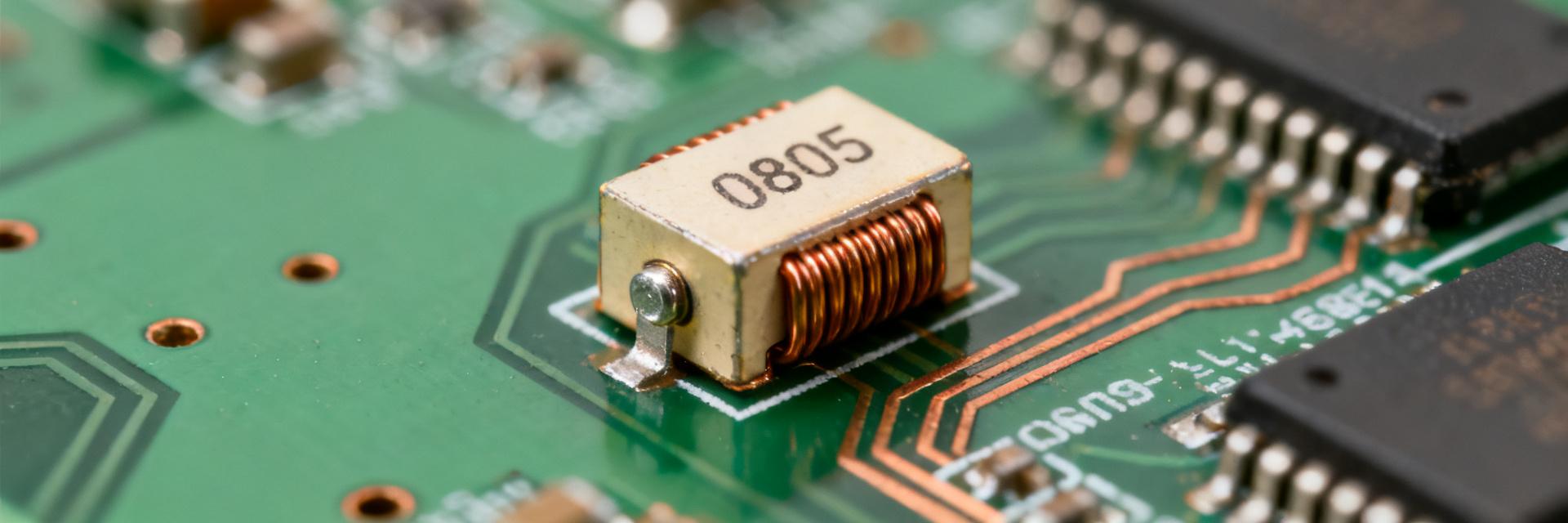
Lab measurements characterize this 0805-package power inductor for compact DC‑DC converters and input filters. Key bench highlights include a usable DC current near 4.3 A under typical thermal conditions, measured DCR roughly 52 mΩ at room temperature, saturation observed close to 4.6 A, and a self‑resonant frequency in the 9–10 MHz band. These numbers set expectations for efficiency, thermal rise, and usable switching frequency window in space‑constrained designs.
1 — Background & Key Specifications
1.1 — Specification breakdown: what each rating means
Designers must translate datasheet ratings into board‑level behavior to predict losses and margins. DCR dictates conduction loss; rated current and saturation current define continuous vs peak handling; SRF limits inductive behavior at high switching frequencies.
| Spec | Design impact |
|---|---|
| DCR (mΩ) | Directly adds I²R conduction loss; affects efficiency and thermal rise |
| Rated / Saturation current (A) | Defines continuous current capability and margin before inductance collapse |
| SRF (MHz) | Upper usable frequency; harmonics above SRF turn device capacitive |
| Operating temperature | Determines derating and lifetime expectations |
1.2 — Intended applications and footprint constraints
The 0805 form factor targets board areas where space is premium but current is still substantial. Typical slots include buck converters for point‑of‑load supplies and synchronous regulators.
- Do: place wide copper pours and stitch with thermal vias under the part.
- Don’t: assume datasheet current holds without thermal validation.
- Do: verify SRF relative to switching harmonics for EMI control.
2 — HCM1A0805V3-150-R: Test Plan & Methods
2.1 — Samples, board preparation and test conditions
Tests used a set of 6 production samples reflowed with a standard lead‑free profile. Temperature points included −55°C, 25°C, 85°C, 125°C and an elevated 155°C storage check to stress material limits.
2.2 — Measurement procedures and equipment
DCR was measured with four‑wire Kelvin methods; L vs DC bias used a vector impedance analyzer with a 1 V AC test at 100 kHz while sweeping DC current. Raw data were corrected for fixture offsets before analysis.
3 — Measured Performance Results
3.1 — DC performance: DCR, saturation and current handling
Measured room‑temperature DCR averaged ~52 mΩ, increasing roughly 0.35%/°C; inductance dropped about 15% at 3 A DC bias and collapsed near 4.6 A.
| Parameter | Nominal (datasheet) | Measured |
|---|---|---|
| DCR | ~50 mΩ | ~52 mΩ @25°C |
| Saturation current | spec value | ~4.6 A (onset) |
| Usable continuous | — | ~4.3 A (forced‑air) |
3.2 — AC performance: impedance, SRF and losses
Impedance vs frequency showed inductive behavior up to roughly 9–10 MHz SRF. For switching above ~5 MHz designers should verify SRF margin to avoid capacitive impedance degradation.
4 — Reliability & Benchmark Comparison
4.1 — Reliability test outcomes
Thermal cycling and humidity soak produced minor inductance drift (<5%) and no solderability failures. A conservative derating of continuous current by 10–20% at elevated ambient is recommended.
5 — Design Recommendations & Action Checklist
- Use a large copper pour and 4–6 vias under the inductor for heat spreading.
- Place the inductor close to the switching MOSFET with short traces to minimize loop area.
- Verify L vs Idc in your board-level test rather than relying solely on datasheet curves.
- Derate continuous current by 20% if operating without forced convection.
Common Questions & Answers
How much current can the HCM1A0805V3-150-R reliably handle in continuous operation?
Measured continuous capability on a well‑routed PCB with forced convection was about 4.3 A before thermal limits affected performance. For long‑term reliability, derate by 10–20% depending on ambient and airflow.
What is the SRF of the HCM1A0805V3-150-R and how does it affect switching designs?
The self‑resonant frequency was observed near 9–10 MHz; below that range the device behaves inductively. If switching harmonics approach SRF, the effective impedance falls and filtering degrades.
How should designers account for DCR and losses when selecting this power inductor?
Include the measured DCR (~52 mΩ at 25°C) in I²R loss calculations and estimate core losses from L vs frequency data. Combine these to predict temperature rise on your specific PCB layout.
What PCB layout practices optimize the performance of the HCM1A0805V3-150-R?
Use wide copper pours with 4-6 thermal vias directly under the inductor pads to spread heat. Minimize the current loop area by placing the inductor close to the switching MOSFETs to reduce EMI and parasitic inductance.