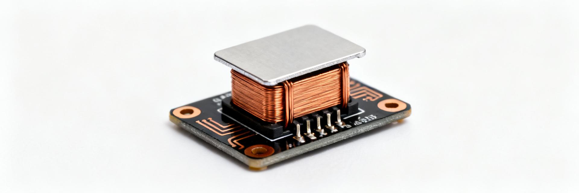
AMELH5030S-2R2MT for Power Supplies: How to Choose & Size
Meta description: "AMELH5030S-2R2MT selection and sizing for reliable, efficient power supply design — practical checks and a worked example."
Switching converters that overheat, show excessive output ripple, or saturate typically trace back to an under‑specified inductor. This guide explains how to evaluate, choose, and size the AMELH5030S-2R2MT for reliable power supply design, with concrete checks and a worked calculation you can replicate on the bench.
The approach below is practical and US‑market focused: direct formulas, a numeric buck example (12V→5V, 3A, 500 kHz), and a downloadable result table you can copy into spreadsheets. Values for Isat, DCR, Irms rating and thermal rise are taken from the datasheet when available; placeholders are used here so you can swap in the official numbers for final verification.
1 — Why the AMELH5030S-2R2MT is relevant to power supplies (background)
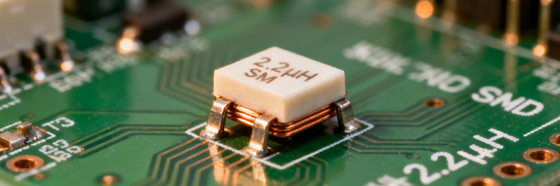
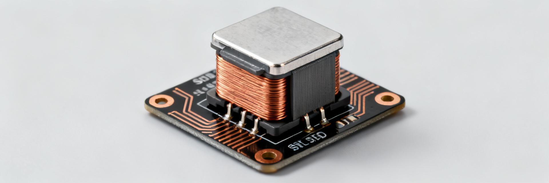
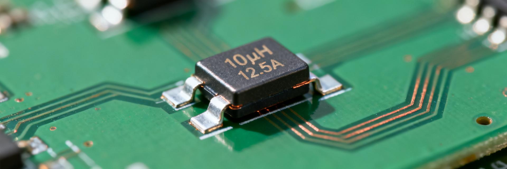
Point: Choose an SMD molded power inductor when you need compact size with reasonable current handling and low electromagnetic emission. Evidence: the part family targets surface‑mount DC–DC converters where board area and reflow compatibility matter. Explanation: for many synchronous buck and boost converters a molded power inductor provides a good tradeoff between power density and manufacturing ease, but you must verify saturation and thermal limits against your worst‑case current and ambient.
1.1 — Key electrical parameters to watch
Point: Extract these datasheet fields and use them in calculations. Evidence: inductance (µH), tolerance, DC resistance (DCR), Isat (saturation current), Irms (rated current), self‑resonant frequency (SRF), temperature rise and max part temperature. Explanation: inductance sets ripple, DCR sets copper loss, Isat limits peak current before core collapse, Irms and thermal rise control steady‑state heating, and SRF indicates usable frequency range.
1.2 — Typical topologies and use cases
Point: This inductor size/type typically fits medium‑power DC–DC converters. Evidence: common use cases include synchronous buck, boost, and SEPIC converters in point‑of‑load and intermediate bus applications. Explanation: molded SMD power inductors offer compact footprint and assembly advantages; choose them when power density and board‑level reflow are priorities, but pick higher Isat or larger packages when saturation margin and lower ripple are critical.
2 — How to calculate required inductance and ripple (data + method)
Point: Use topology‑specific formulas to derive ΔIL and required L. Evidence: standard derivations below produce peak‑to‑peak ripple consistent with inductor volt‑second balance. Explanation: pick a target ΔIL (percent of Io) based on output capacitor ESR and transient goals, then solve for L or compute ΔIL for a candidate inductor.
2.1 — Formulae for common topologies (buck & boost)
Buck: ΔIL = (Vin − Vout) * D / (L * fs)
Where D = Vout / Vin, fs = freq, L = inductance.
Boost: ΔIL = Vout / (L * fs) * (1 − D)
Where D = 1 − Vin/Vout.
2.2 — Target ripple selection & design tradeoffs
Point: Select ΔIL as a percent of Io to balance transient response and loss. Evidence: common targets are 20–40% of Io depending on output cap ESR and transient requirements. Explanation: lower ripple reduces output voltage excursion and EMI but increases required L (larger part or higher cost) and may reduce power density. Higher ΔIL raises Irms and conduction loss, increasing temperature; factor DCR into this tradeoff.
3 — Current, saturation and thermal checks (data analysis)
Point: Verify Ipk vs Isat and compute Irms and conduction loss. Evidence: formulas below convert ΔIL into peak and RMS currents for component checks. Explanation: meeting Isat and Irms ratings with margin prevents saturation and excessive heating under worst‑case duty and ambient.
3.1 — Saturation & RMS Check
Compute peak inductor current for buck: Ipk = Iout + ΔIL / 2. Compare Ipk to Isat (20–30% margin). For RMS: Irms = sqrt(Iout² + (ΔIL²)/12).
3.2 — Power Loss
P_DCR = Irms² × DCR. Estimate temp rise from datasheet. Aim for conduction loss < 10–20% of total converter losses by selecting lower DCR.
4 — Step-by-step sizing example (Worked Calculation)
4.1 — Case Study: Buck 12V→5V, 3A, fs = 500 kHz
4.2 — Decision outcome & alternatives
Point: If checks fail, adjust topology or part. Evidence: options include raising L, paralleling inductors, selecting a higher‑Isat part, reducing fs, or changing package. Explanation: increasing L lowers ΔIL but may increase size; paralleling splits current but doubles layout complexity.
5 — PCB layout, mechanical & thermal considerations
5.1 — Placement and thermal management
Place the inductor close to the switching node with short, wide traces for high‑current paths. Use thermal vias beneath adjacent copper areas for heat spread, keep the inductor isolated from hot MOSFETs, and maximize copper pour for conduction. Airflow and board copper are the cheapest ways to reduce temperature rise.
5.2 — Mechanical, footprint and assembly notes
Check the recommended land pattern and reflow profile; molded power inductors can be sensitive to board warpage and mechanical shock. Confirm component height fits enclosure and that pick‑and‑place and reflow processes match vendor recommendations to avoid tombstoning or solder fatigue.
6 — Final selection checklist & SEO/production notes
6.1 — Quick selection checklist
- Required inductance (calculated L) and tolerance.
- Maximum DCR to meet efficiency goals.
- Isat with 20–30% safety margin.
- Irms rating for continuous current.
- BOM callouts: place part number for assembly engineers.
6.2 — SEO Keywords
Primary placement: AMELH5030S-2R2MT in title and intro. Use "power supply design" and long-tail phrases like "how to size 2.2 µH power inductor for SMPS".
Summary
- ✔ Follow a repeatable workflow: extract datasheet numbers, compute required L and ΔIL, and verify Isat/Irms and DCR losses.
- ✔ Use topology formulas to set a target ΔIL (20–40% of Io typical), solve for L, and compare ratings with a 20–30% safety margin.
- ✔ Practical checks include estimating P_DCR, confirming thermal rise, and validating layout/assembly constraints.
Additional notes for the writer (concise)
Provide one downloadable table containing datasheet key values and computed example results. Keep US tone: direct and data‑driven.
| Parameter | Placeholder / Example Result |
|---|---|
| Inductance (L) | 2.2 µH (candidate) / required ≈ 6.48 µH |
| ΔIL (target) | 0.9 A (30% of 3 A) |
| ΔIL (with 2.2 µH) | ≈ 2.65 A |
| Ipk | ≈ 4.33 A |
| Irms | ≈ 3.10 A |
| DCR (placeholder) | 0.03 Ω |
| P_DCR | ≈ 0.29 W |
| Isat (datasheet) | — replace with datasheet value and verify margin |