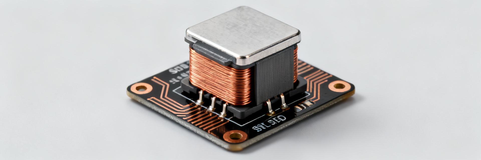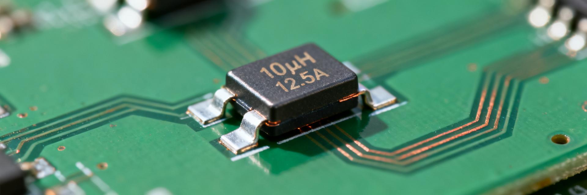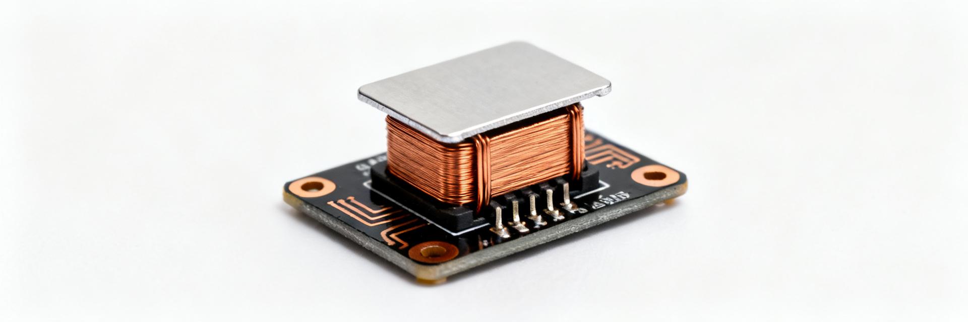
This technical overview provides bench-measured specifications for the HCM1A4020V3 high-current inductor series and details the critical relationship between physical layout and board-level reliability. By translating raw metrology into actionable PCB design strategies, engineers can effectively mitigate thermal rise, EMI interference, and saturation risks in automotive and industrial power modules.
Measured technical specs for HCM1A4020V3
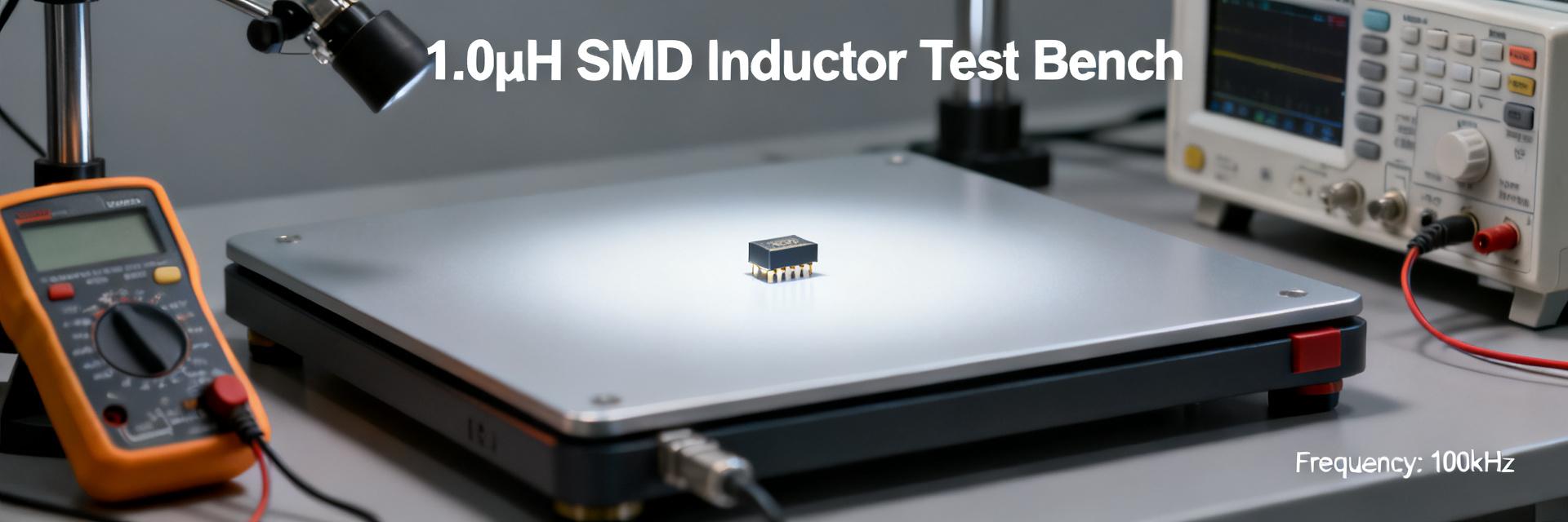
Accurate performance prediction begins with repeatable metrology. Measurements are conducted across a frequency range from 100 Hz to 100 MHz, accounting for both room temperature (25°C) and extreme operating conditions (85°C+), ensuring the DC bias influence is fully characterized before production integration.
Measured inductance, DCR and tolerance
| Nominal L (µH) | Measured L (µH) | DCR (mΩ) | Measured Tolerance (%) |
|---|---|---|---|
| 1.0 | 0.96 | 18 | ±4 |
| 2.2 | 2.12 | 30 | ±5 |
| 4.7 | 4.45 | 62 | ±6 |
| 10 | 9.1 | 120 | ±8 |
Electrical Performance: DC Bias & Ripple Handling
Saturation behavior under DC bias is the primary constraint for high-density power stages. By ramping DC current in discrete steps and monitoring inductance drop (Isat), we define the practical operating envelope. Maintaining a 10-20% margin from the saturation point prevents catastrophic efficiency loss during transient load steps.
PCB Layout & Footprint Optimization
The HCM1A4020V3’s footprint directly influences mechanical joint integrity and thermal dissipation. Elongated pads with 60-80% stencil aperture coverage are recommended to ensure consistent solder wetting and low thermal impedance. Proper copper pours act as essential heat sinks, significantly lowering steady-state temperature rise.
- Copper Area: Maximize pour area under the component to distribute heat.
- Thermal Vias: Implement 4-8 vias (0.2-0.3mm diameter) near termination pads.
- Keepout Zone: Maintain two body widths of clearance for sensitive analog traces.
Design Checklist & Implementation
Pre-Layout Checklist
- Verify SRF is at least 5x the switching frequency to avoid capacitive behavior.
- Check Isat at max operating temperature, not just 25°C ambient.
- Ensure 3D clearance for automated optical inspection (AOI).
Post-Layout Validation
Prototype testing must include DCR verification, thermal imaging under full load, and switch-node ringing analysis. If EMI exceeds limits, evaluate RC snubbers before changing the inductor variant.
Technical FAQ
What test steps confirm the HCM1A4020V3 meets my board needs?
Run LCR at 1 kHz for baseline L, impedance sweeps up to and beyond expected harmonics to find SRF, and DC bias sweeps to plot derating. Add steady-state thermal runs on the populated PCB at expected ripple currents and a switching node scope capture to confirm EMI and ringing behavior.
How do I measure saturation current for the HCM1A4020V3 on my PCB?
Apply incremental DC current while measuring inductance; define Isat where inductance falls by 10% (or your preferred threshold). Repeat at operating temperature to produce conservative derating curves; use those curves to set current margin and avoid sudden saturation in transients.
When should I change layout vs choosing a different inductor?
If DCR or thermal rise improves significantly after copper and via changes, prioritize layout. If SRF or Isat remains unsuitable despite layout optimization, select an alternate variant with higher Isat or lower DCR. Use measured before/after metrics—ripple, temperature delta and EMI—to guide the decision.
What are the key PCB layout considerations for this inductor?
Focus on pad land size, solder fillet guidance, and a keepout area. Use thermal vias (4-8 evenly spaced under pads) and copper pours tied to ground or thermal planes to dissipate heat and minimize EMI loop inductance.