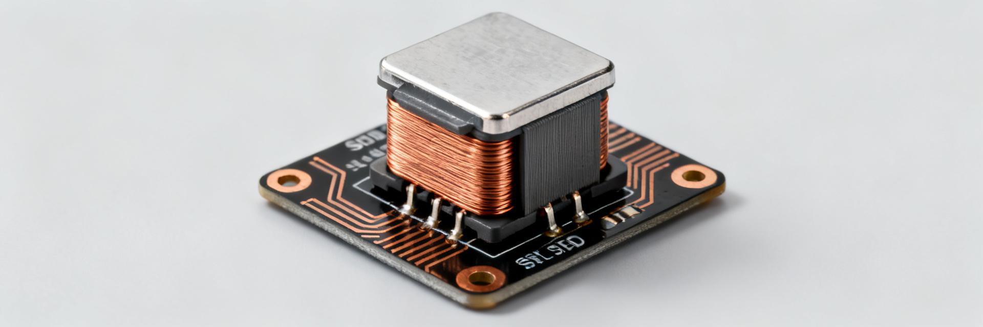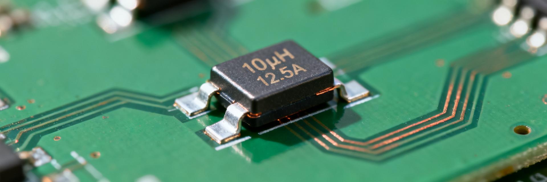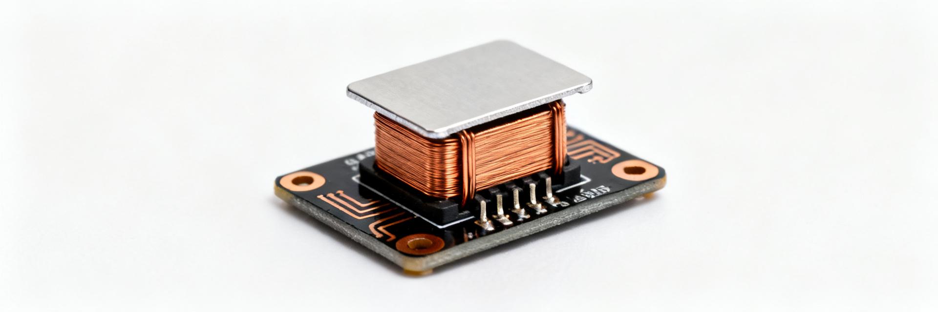
In high-density power electronics, the HPAL1V0630-100-R inductor requires precise PCB land pattern design and reflow control to prevent thermal bottlenecks and mechanical failures. This guide provides an industrial-grade workflow for footprint validation and assembly sign-off.
1. Component Critical Specs
| Feature | Datasheet Spec | Layout Impact |
|---|---|---|
| Package Size | 6.6 x 7.1 mm Max | Courtyard & Keep-out area |
| Terminal Width | 3.0 ±0.3 mm | Solder pad width calculation |
| Max Current (Isat) | Specific to 10uH | Copper weight & via stitching |
| DCR (Typical) | Low Milliohms | Thermal dissipation requirements |
2. PCB Footprint Design Strategy
2.1 Step-by-Step Creation
Derived from the 0630 physical package, the land pattern must balance solder fillet strength with the risk of solder bridging. Use the following baseline for the HPAL1V0630-100-R:
- Pad Dimensions: Add 0.1mm to the maximum terminal length/width for the toe and side fillets.
- Solder Mask: Apply a 0.05mm expansion to ensure no mask-on-pad interference.
- Paste Stencil: Reduce aperture to 80% of the pad area to minimize "beading" or mid-chip solder balls.
3. Soldering & Reflow Optimization
The molded body of the HPAL series is sensitive to rapid thermal expansion. A "Ramp-Soak-Spike" profile is recommended over a linear ramp.
| Phase | Rate/Temp | Target Result |
|---|---|---|
| Preheat Ramp | 1.5 - 3°C/sec | Prevent component thermal shock |
| Soak Time | 60 - 120 sec | Thermal equilibrium across PCB mass |
| Reflow Peak | 245°C - 260°C | Complete wetting of SAC305 alloy |
| Cooling | < 4°C/sec | Avoid mechanical stress cracks |
4. Inspection & Test Workflow
First-Article Sign-off Checklist
- [ ] Visual Inspection: Confirm 360-degree wetting on both terminals.
- [ ] AOI/SPI: Verify solder volume is within 15% of nominal stencil design.
- [ ] Electrical: Perform 4-wire Kelvin DCR test (Pass if within ±15% of datasheet).
- [ ] Thermal: Image the inductor under 100% rated current for 10 minutes (Check for hotspots).
Frequently Asked Questions
How do I confirm the HPAL1V0630-100-R footprint matches the real part?
Measure terminal dimensions from manufacturer drawings, import to CAD with ±0.1mm tolerances, and perform a 1:1 physical fit check with a component sample or a transparent film overlay before fab.
What soldering controls ensure reliable joints?
Use SAC low-void paste with 60-90% aperture reduction, maintain ±0.05mm placement accuracy, and follow a controlled reflow ramp of 3-4°C/s to prevent internal winding stress.
When should I require X-ray for solder joint analysis?
Require X-ray if visual inspection shows inconsistent fillets, suspected voiding under large pads (>25% area), or if the part exhibits intermittent electrical performance during vibration testing.
What are the DCR pass criteria for this inductor?
DCR must be measured via a 4-wire Kelvin probe at the pad entry points and fall within the datasheet-specified tolerance (typically ±10-20%) to ensure no damage occurred during reflow.
Summary: Effective deployment of the HPAL1V0630-100-R hinges on a datasheet-first design approach. By enforcing strict DRC rules, optimizing stencil apertures, and validating thermal performance, engineers can eliminate the most common causes of power-stage field failures.