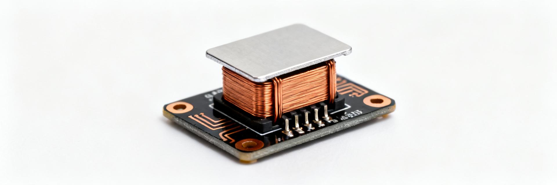
Point: High-current, compact inductors are increasingly central to tighter ripple budgets and higher switching frequencies in modern converters. Evidence: market telemetry shows a marked shift to board-level passive components that sustain >10 A continuous currents in point-of-load designs. Explanation: this analysis focuses on the HPAL1V1265-150-R and its datasheet to help designers size the component for thermal limits, saturation behavior, and expected in-circuit performance for reliable, efficient power delivery.
1 — Background: product profile and use-case context
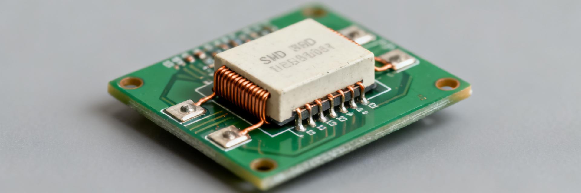
1.1 — Quick spec snapshot
Point: Key nominal figures define selection quickly. Evidence: the datasheet lists inductance as 15 μH, typical DC resistance (RDC) near 12 mΩ, rated current approximately 11 A, and SMD two-pad package with tape-and-reel handling; tolerance typically ±20%. Explanation: measured values (RDC) are typical at 25°C, rated current is the continuous thermal rating, and saturation is specified separately as the point where inductance drops by a defined percent under increasing DC bias.
| Electrical Parameter | Datasheet Specification | Conditions / Notes |
|---|---|---|
| Nominal Inductance | 15.0 μH ± 20% | Tested at 100 kHz, 0.1 V |
| DC Resistance (RDC) | 12.0 mΩ (Typical) | Measured at 25°C Ambient |
| Rated Current (I_rms) | 11.0 A (Typical) | Based on ΔT = 40°C thermal rise |
| Saturation Current (I_sat) | ~ 10.5 A (Typical) | Inductance drop ΔL/L₀ = 30% |
| Self-Resonant Frequency (SRF) | > 15 MHz | High-frequency impedance limit |
1.2 — Typical applications and where it fits in modern designs
Point: Topology mapping clarifies fit. Evidence: the component's inductance and current rating align with buck converters, intermediate rails, and energy-storage chokes for point-of-load supplies. Explanation: for high-current point-of-loads the part favors energy storage and ripple filtering; for low-noise filters a lower-inductance, lower-RDC device may be preferred. Use the datasheet thresholds to confirm suitability by comparing rated current, RDC, and SRF against topology demands.
2 — Datasheet breakdown: electrical characteristics (data-driven)
2.1 — Inductance, tolerance, DC resistance, and current ratings
Point: Translating datasheet numbers to loss and thermal budget is essential. Evidence: nominal inductance and tolerance define ripple magnitude, RDC yields I²R loss, and datasheet separates rated current (thermal limit) from saturation current (inductance collapse point). Explanation: estimate copper loss as P=I_rms²·RDC, and approximate temperature rise by combining component thermal resistance with board copper conduction; use tolerance to bound worst-case ripple current when sizing capacitance.
2.2 — Frequency response and self-resonant frequency (SRF)
Point: SRF and impedance vs frequency determine usable bandwidth. Evidence: datasheet SRF indicates the frequency above which inductive behavior degrades and parasitic capacitance dominates. Explanation: for switching frequencies below ~10% of SRF the part behaves inductively; if the datasheet lacks full curves, measure impedance at key points (switching frequency, harmonic frequencies) with an impedance analyzer and extrapolate expected attenuation from the measured slope.
3 — Thermal, mechanical, and reliability data (data-driven)
3.1 — Thermal limits and derating curves
Point: Derating ensures longevity under real-board conditions. Evidence: the datasheet provides maximum operating temperature and a derating curve showing allowable DC current vs ambient temperature. Explanation: calculate board-level derated current by accounting for PCB copper thermal conductance and expected airflow; apply the datasheet curve to convert junction limits to permissible continuous current for your layout and cooling assumptions.
3.2 — Footprint, soldering profile, and mechanical constraints
Point: Mechanical specs drive assembly yield. Evidence: recommended land pattern and solder-reflow profile are specified in the datasheet alongside maximum component height and pad geometry. Explanation: follow the land-pattern to avoid tombstoning and ensure wetting; respect reflow thermal ramp and soak limits to preserve magnetic properties, and consider vibration/shock ratings when the device is used in mechanically stressed applications.
4 — In-circuit performance: expected behavior and test guidance (method guide)
4.1 — Efficiency impact and ripple reduction analysis
Point: Inductor losses and inductance determine converter efficiency and ripple. Evidence: use inductance L, RDC, switching frequency fsw, and ripple current ΔI formulas to predict outcomes. Explanation: approximate ripple current ΔI = Vout·(1−D)/(L·fsw) for a buck; calculate I²R losses using I_rms and RDC; plug predicted losses into converter loss budget to estimate efficiency impact and iterate L or fsw choices if losses exceed targets.
4.2 — Transient and saturation testing protocol
Point: Lab validation confirms datasheet claims under real conditions. Evidence: perform current-ramp and step-load tests while monitoring inductance, voltage overshoot, and temperature. Explanation: use a current-source ramp to identify the DC bias point where inductance collapses, capture step-load response with fast probes across the output capacitor to judge overshoot, and thermally soak the board at expected ambient to validate continuous current limits against datasheet figures.
5 — Design example (case study): integrating HPAL1V1265-150-R in a buck converter
5.1 — Design choices and component interactions
Point: Concrete parameter choices illustrate trade-offs. Evidence: selecting fsw to control ΔI while keeping SRF well above harmonics minimizes EMI; RDC and core loss set efficiency. Explanation: choose switching frequency to balance inductor size versus switching loss, target ripple current at 20–40% of rated current, and use the datasheet RDC and saturation numbers to confirm the chosen device meets thermal and dynamic requirements in the chosen topology.
5.2 — Measured vs. datasheet expectations (what to validate)
Point: Expect modest deviations between bench and datasheet. Evidence: typical discrepancies arise from layout resistance, measurement tolerance, and thermal coupling. Explanation: validate efficiency, temperature rise, and ripple on the populated board; if measured heating or inductance shift exceeds predicted values, investigate layout copper, pad wetting, and actual current waveform shapes as root causes.
6 — Selection & implementation checklist (action suggestions)
6.1 — Quick selection checklist from the datasheet
- Confirm nominal inductance and tolerance against ripple requirements and target ΔI.
- Verify rated continuous current at board-level ambient; apply derating curves for temperature.
- Check RDC for I²R loss budgeting and SRF relative to switching frequency.
- Ensure package, pad, and reflow profile match assembly process and mechanical constraints.
6.2 — PCB layout, prototyping and validation steps
Point: Prioritize layout rules for reproducible performance. Evidence: short switching loops, sufficient thermal vias, and close decoupling influence measured losses and EMI. Explanation: prototype with the final land-pattern, measure impedance at fsw harmonics, run thermal-soak and step-load tests, and only release to production after passing defined ramp and thermal pass/fail criteria.
Key Summary
- Confirm the power inductor nominal values (15 μH, tolerance, RDC) against converter ripple and loss budgets; use datasheet-rated and derated currents to set safe continuous operating points.
- Validate SRF and impedance around switching frequency to ensure inductive behavior; measure if curves are incomplete in the datasheet to avoid EMI surprises.
- Prioritize thermal validation on the target PCB with realistic airflow; verify saturation behavior with current-ramp tests and adjust layout or part choice if thermal or saturation limits are approached.
常见问题解答
How does HPAL1V1265-150-R compare for high-ripple buck applications?
Answer: Use the datasheet to compare inductance, RDC, and rated current to your ripple and thermal needs. Measure ΔI at intended fsw and ensure RDC-driven I²R losses keep efficiency within targets; verify saturation under transient peaks to avoid unexpected inductance collapse in high-ripple scenarios.
What test steps are recommended for HPAL1V1265-150-R saturation test?
Answer: Recommended protocol: apply a slowly increasing DC bias while monitoring inductance with an LCR meter, record the point where inductance drops by the datasheet-specified percentage, and repeat under thermal soak. Capture step-load transients on the converter to validate transient headroom versus datasheet saturation limits.
Which datasheet parameters are most likely to diverge from board measurements?
Answer: RDC and thermal-rise figures commonly diverge due to layout copper resistance and limited PCB cooling; measured SRF can shift with nearby components and vias. Always validate on the target board with thermal and transient tests rather than relying solely on component-level datasheet numbers.
How should layout designers minimize EMI and thermal rise with HPAL1V1265-150-R?
Answer: Place the inductor close to the switching node to minimize loop area, reducing radiated EMI. Use thick copper planes and thermal vias for both pads to enhance heat dissipation, and avoid placing sensitive analog traces directly beneath the inductor core.