Facing overheating or solder-joint failures when integrating the HPAL1V0650-2R2-R on your board? This concise guide gives solution-oriented PCB mounting and thermal tips you can apply now to keep the 2.2 µH, high-current SMD inductor stable and reliable in production designs. Refer to the manufacturer datasheet for exact pad dimensions, peak temperature limits, and current-derating curves before committing to a final layout.
Point: early design choices determine long-term reliability. Evidence: the part’s rated current (≤11 A) and DC resistance set I²R loss; core losses add under switching. Explanation: treat the device as both a conductor and a localized heat source—layout and assembly choices (pad geometry, copper, vias, reflow) control junction rise and solder-joint fatigue.
1 — Background: key specs & why layout matters
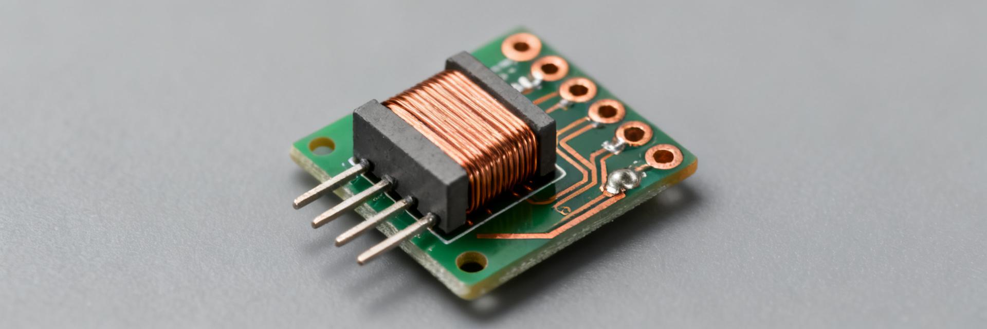
What to check in the HPAL1V0650-2R2-R datasheet
Point: datasheet is the single-source truth. Evidence: key values to extract are rated current (≤11 A), DC resistance, recommended reflow profile, and recommended land pattern. Explanation: use those numbers to size copper, choose paste coverage, and set thermal test currents; for example, use the rated current for continuous heating tests and derating curves for pulse scenarios.
Actionable direction: always cross-check peak temperature and current-derating curves before final placement; verify recommended solderable landing size vs. your stencil vendor and IPC guidelines.
How inductor thermal behavior affects nearby components
Point: inductors create heat via I²R and core losses. Evidence: measured temp rise commonly appears at pads and adjacent traces leading to solder fatigue and delamination over cycles. Explanation: identify heat-sensitive ICs, capacitors, and plastic connectors within the inductor’s thermal footprint and apply minimum clearances or barriers.
Actionable direction: map a 10–15 mm (0.4–0.6 in) exclusion zone for the hottest components, or add thermal barriers such as grounded copper pour or silicon isolators if space is tight.
2 — PCB footprint & mounting best practices
Recommended footprint and pad geometry
Point: reliable fillet formation is key to solder-joint life. Evidence: two rectangular pads with solder-mask-defined (SMD) lands encourage fillet menisci and reduce tombstoning. Explanation: design paste aperture at ~60–80% paste coverage per pad area to avoid excess solder; align pad length with manufacturer outline while allowing 0.1–0.2 mm (0.004–0.008 in) assembly tolerance.
- Checklist for footprint verification: pad solderability, SMD vs NSMD choice, stencil aperture % (start 65%), and fillet visibility on inspection.
- Actionable direction: run a 1:1 PCB print with stencil vendor for first build; adjust apertures after cross-section inspection.
Placement, routing and current-carrying considerations
Point: minimizing loop area reduces loss and EMI. Evidence: wide, short traces and copper pours carry the high DC current with lower I²R loss and reduce switching-node inductance. Explanation: orient the inductor so high-current traces exit on the short side; place bulk and decoupling capacitors adjacent to the switch node to shorten loop length.
Actionable direction: use a trace-width calculator for continuous currents ≥ rated current (11 A); when possible, tie pads to internal power planes with 2–6 thermal vias to spread current and heat.
| Current | Suggested single-layer width (1 oz) | Notes |
|---|---|---|
| 11 A | ~4.5 mm (0.18 in) | Use wider or parallel traces; prefer copper pour |
3 — Thermal management techniques
Copper area, pours and thermal vias
Point: copper is the primary heat sink on a PCB. Evidence: expanding copper area and adding vias under pads shifts heat into planes and reduces localized temperature rise. Explanation: using a staggered via grid improves conduction; plated through vias with adequate annulus minimize thermal resistance to internal planes.
Actionable direction: start with 2–6 vias per pad to plane(s), spaced evenly under the pad edge, then iterate with thermal testing. Consider 2–3 oz copper for high-power runs if budget permits.
Airflow, spacing and enclosure strategies
Point: convection and forced airflow dramatically change equilibrium temperature. Evidence: moving from natural convection to a low-flow fan can lower junction temperatures by double-digit °C in many boards. Explanation: allow airflow channels and orient the board for consistent convection paths within the enclosure.
Actionable direction: reserve 1–2 mm (0.04–0.08 in) clearance around the inductor for airflow; in tight enclosures, plan for small board-level fans or attach the inductor area to a chassis plate via a thermally conductive pad.
4 — Assembly & validation: soldering, reflow and thermal testing
Reflow profile & solder-joint reliability
Point: improper reflow reduces solder-joint life. Evidence: excessive peak temperature or prolonged dwell increases intermetallic growth and weakens joints. Explanation: follow the device-recommended ramp rates and peak temperature; prefer shorter peak dwell consistent with the lead-free profile the datasheet specifies.
Actionable direction: validate your process with IPC solderability checks and cross-section inspection on first articles; record ramp rates and peak temps for traceability.
Thermal validation methods and test plan
Point: controlled thermal testing quantifies margins. Evidence: steady-state heating, IR thermography, and thermocouple measurements reveal hot spots and time constants. Explanation: a systematic matrix exposes both equilibrium and fatigue behaviors under realistic duty cycles.
Actionable direction: use a thermal test matrix (0.5×, 1.0×, 1.25× rated current) and record temp rise after 10–30 minutes; include power-cycling and solder-joint microsections in qualification sampling.
5 — Two short use-case examples + quick checklist
Example A: high-current buck regulator PCB
Point: targeted layout changes reduce inductor temperature and improve reliability. Evidence: in a typical buck layout, replacing narrow traces with wide pours and adding six thermal vias under the inductor pad noticeably reduced perceived temperature and the switching node noise. Explanation: short high-current loops and adjacent bulk capacitors reduce both thermal and EMI stress.
Actionable direction: keep the cap adjacent to the switch node, route input and return as wide pours, and add multiple vias under the inductor pad to internal planes for both heat and current sharing.
Quick design & production checklist
- Datasheet review: extract rated current, DC R, land pattern, reflow spec.
- Footprint validation: stencil % and fillet inspection.
- Trace-width check: calculate for ≥11 A continuous.
- Copper & via plan: 2–6 vias/pad, consider 2–3 oz copper.
- Assembly check: follow reflow profile; perform cross-section tests.
- Thermal test: IR scan, thermocouple readings at 0.5×/1.0×/1.25× currents.
- Production sampling: solder-joint microsections and max temp pass/fail.
Summary
Practical integration depends on deliberate footprint design, robust copper and via-based thermal paths, and a focused validation plan. The HPAL1V0650-2R2-R requires treating layout and assembly as thermal design tasks: prioritize datasheet limits, minimize high-current loop area, and validate with thermal imaging and controlled current tests before production.
- Prioritize datasheet limits and land-pattern specs when creating the HPAL1V0650-2R2-R PCB footprint and stencil; mismatches cause solder and thermal issues.
- Use wide traces, copper pours, and 2–6 thermal vias per pad to spread heat into internal planes; consider thicker copper for heavy currents.
- Validate with a thermal test matrix (0.5×, 1.0×, 1.25× rated current), IR imaging, and solder-joint cross-sections to confirm reliability before mass production.
Frequently Asked Questions
How should I size PCB traces for high-current SMD inductors?
Use a trace-width calculator for continuous current equal to or above the rated 11 A; where space is limited, use parallel traces or copper pours. Prefer internal planes or multiple layers to distribute current and lower I²R loss, and verify by measuring PCB resistance in-circuit.
What stencil coverage is recommended for inductor pads to ensure good fillets?
Start at ~65% paste coverage per pad area and adjust based on cross-section. Too much paste causes solder bridging; too little creates weak fillets. Validate with a first-article assembly and inspect solder fillets under magnification.
Which thermal validation methods are effective for inductor reliability testing?
Combine steady-state current heating, IR thermal imaging, and thermocouple readings near pads. Include power-cycling tests to reveal solder fatigue; record temperature after an equilibrium period (10–30 minutes) for each test current.
What are the key thermal specifications for the HPAL1V0650-2R2-R inductor?
The inductor features a rated current of up to 11 A and a 2.2 µH inductance. Its power losses are driven by DC winding resistance (I²R) and AC core losses, requiring careful thermal design to prevent solder joint degradation.