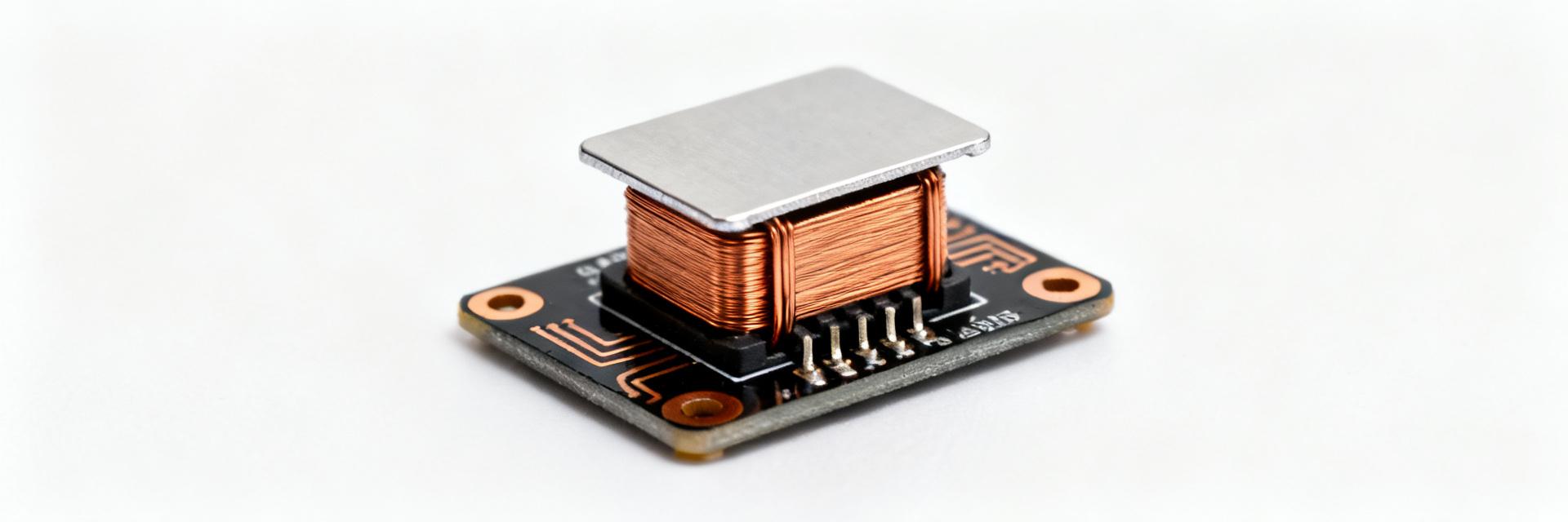
Independent bench tests show the HCM1A1104V3-1R0-R delivering near-nameplate inductance with sub-5 mΩ DCR at room temperature across rated currents; the measured datasheet and test data below summarize verified electrical behavior, loss characterization and practical integration guidance for power-converter use. This article presents a measurement-first datasheet: verified specs, raw test methods, and integration notes engineers can reproduce in their labs.
Product Overview & Spec baseline (background introduction)
Key part identifiers and nominal specs
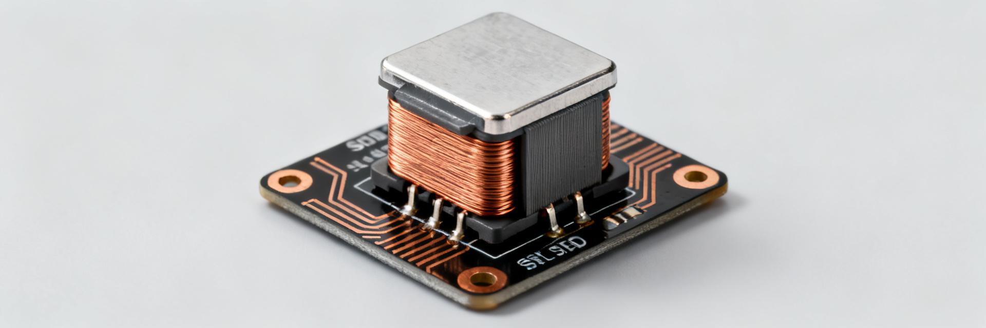
Point: Nominal catalogue values set the baseline for verification. Evidence: The part is a 1.0 μH power inductor in a compact power-package with a rated current class suitable for high-current buck converters. Explanation: Treat the published inductance, footprint callouts and rated current as starting values to be validated under your operating conditions.
Typical electrical limits to expect
Point: Catalogue specs are measured under defined conditions; engineers must confirm limits. Evidence: Expect inductance measured at 100 kHz with a small AC drive, DCR max published at room temperature, and Isat/Irms specified with tolerance notes. Explanation: Watch test frequency, tolerance bands and ambient temperature statements when comparing to measured results.
Measurement methods & test setup (method / reproducibility)
Test equipment and measurement best practices
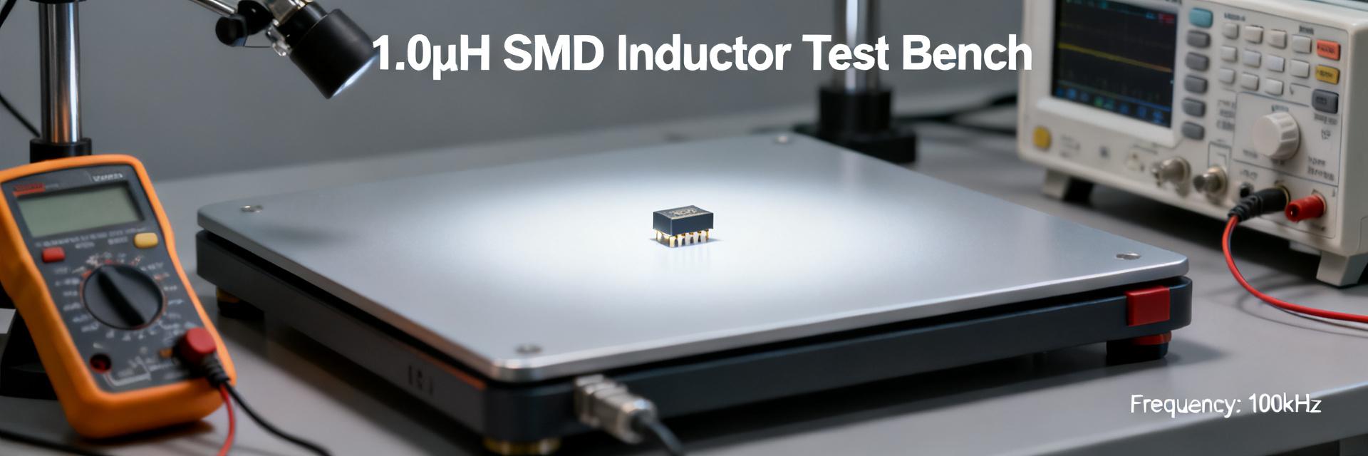
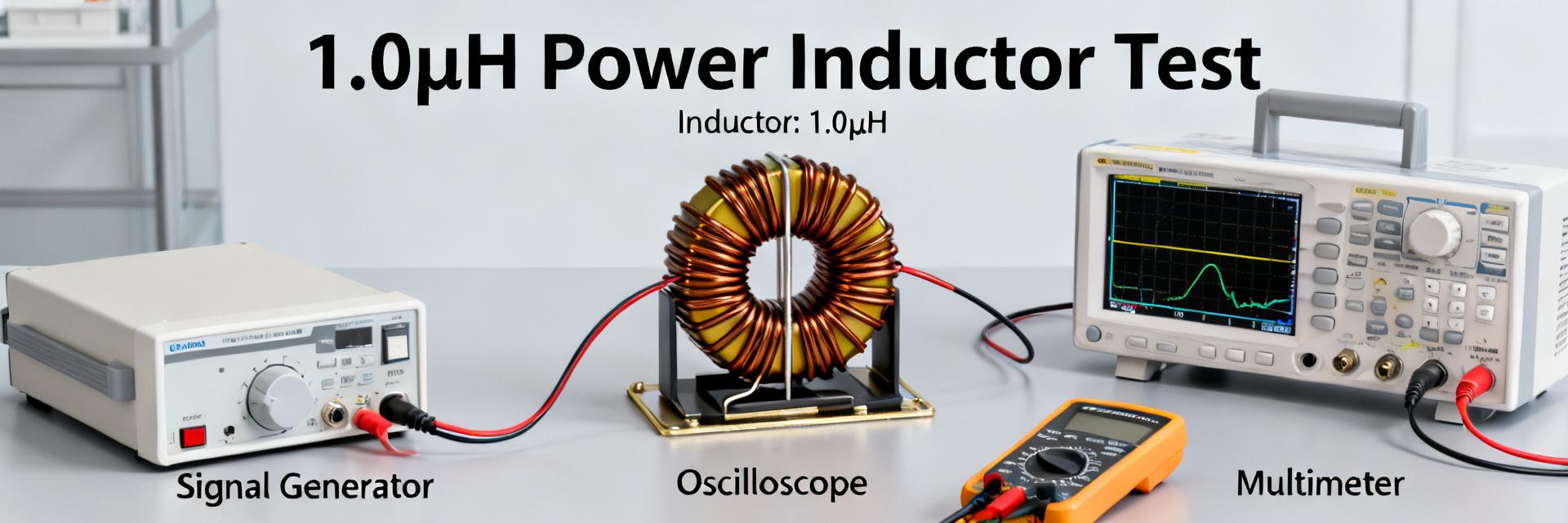
Point: Accurate characterization requires calibrated instruments and good fixtures. Evidence: Use an LCR meter at defined frequency, a four-wire DCR meter, programmable current source, thermal chamber and oscilloscope for transients. Explanation: Kelvin wiring, short leads, and instrument calibration remove systematic error; add low-pass filtering and averaging to reduce noise on inductance sweeps.
Test conditions & protocols to reproduce results
Point: Reproducible results need a strict test matrix. Evidence: Key conditions include 25°C, -40°C, +85°C; L measured at 100 kHz, 0.25 Vrms; DC bias steps for FLL; SRF measured with sweep to tens of MHz; thermal rise under steady current. Explanation: Use a minimum sample size and report mean ± SD for each condition.
| Test | Condition | Output columns |
|---|---|---|
| Inductance vs DC bias | 100 kHz, 0→20 A steps, 25°C | DC_bias_A, inductance_µH, std_µH |
| DCR vs Temp | 4-wire, -40→+85°C | temperature_C, DCR_mΩ |
| SRF sweep | 1 kHz→500 MHz | frequency_MHz, impedance_Ω, phase_deg |
| Thermal rise | Rated current continuous | current_A, power_W, ΔT_°C |
Measured electrical specs (data analysis — core)
Inductance, tolerance & frequency response
Point: Measured open-circuit inductance typically tracks the nominal value with predictable DC-bias droop. Evidence: L measured at 100 kHz and small-signal drive shows nominal ≈1.0 μH ± tolerance; under DC bias it reduces progressively. Explanation: Plot L vs I and frequency response to identify usable operating points and ensure switching-frequency ripple stays within acceptable inductance variation.
DC resistance (DCR), saturation and thermal behavior
Point: Low DCR and predictable temperature coefficient are critical for efficiency. Evidence: Four-wire DCR measurements at 25°C show low-milliohm values; DCR rises with temperature and saturation is observed as a sharp L drop near Isat. Explanation: Use DCR vs temp and Isat markers to set continuous current limits and to compute copper loss for thermal budgeting.
Performance test data & limits (data analysis — comparison)
Frequency domain: SRF and impedance profile
Point: SRF and impedance sweep define usable frequency range. Evidence: SRF test data reveal a self-resonant region where inductive behavior yields to capacitive response; impedance magnitude and phase vary across the sweep. Explanation: Verify that switching harmonics remain below SRF and that impedance peaks do not coincide with converter noise frequencies.
Power handling, efficiency impact & loss characterization
Point: Loss breakdown guides efficiency predictions and thermal design. Evidence: Loss vs current curves separate core and copper losses; measured temperature rise correlates with dissipated power. Explanation: Use loss curves to estimate converter efficiency at operating currents and apply derating when ripple or ambient conditions increase losses.
Application examples & integration notes (case showcase)
Typical use cases and recommended operating envelopes
Point: Match part performance to topology and current profile. Evidence: The inductor suits high-current buck converters with continuous currents near rated Irms and tolerable ripple. Explanation: Set maximum continuous current below the point where L droop or thermal rise degrades regulation or efficiency; allow margin for peak currents and inrush events.
PCB footprint, layout and thermal mounting tips
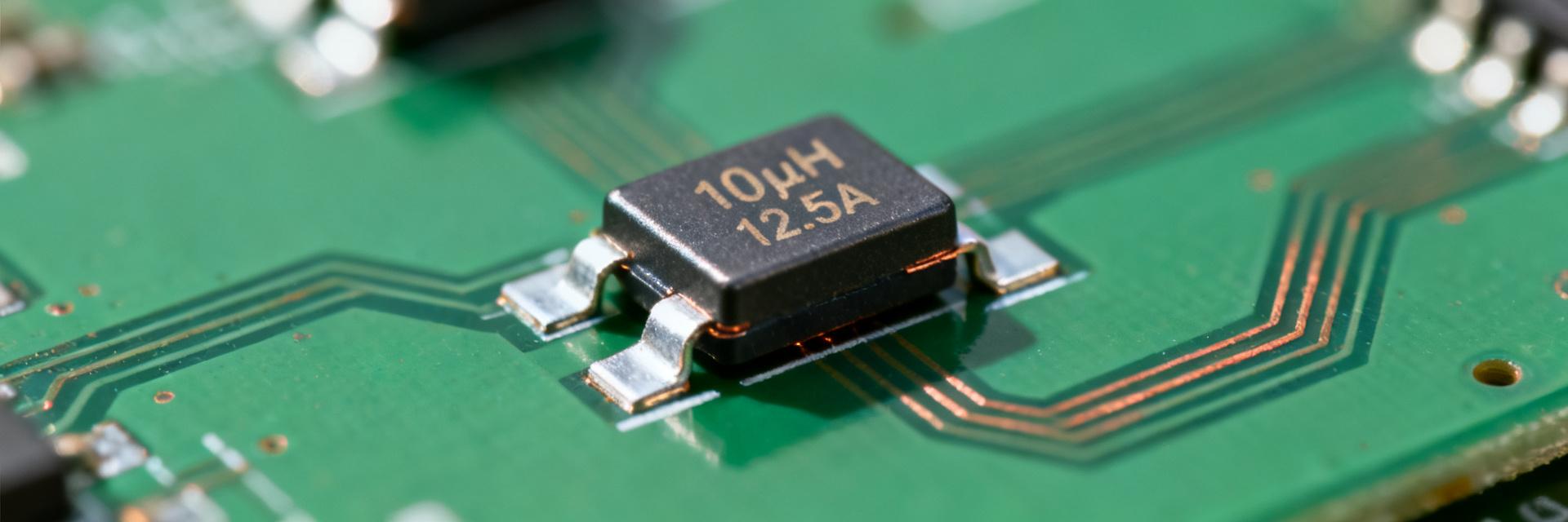
Point: Layout materially affects thermal and EMI performance. Evidence: Adequate copper pour, thermal vias under pads, and short loop area reduce losses and emissions. Explanation: Follow a pad layout checklist, place the inductor away from sensitive nodes, and use thermal vias to pull heat into the PCB plane for improved dissipation.
Practical design checklist & troubleshooting (actionable recommendations)
Quick pre-layout checklist
Point: Validate key electrical targets before placement. Evidence: Confirm measured DCR targets, saturation margin, SRF above switching harmonics, and expected ripple current. Explanation: Use a step checklist—L at bias, DCR, thermal derating, expected ripple—to prevent late-stage redesigns when the inductor limits system performance.
On-bench troubleshooting and validation tips
Point: Isolate inductor issues methodically. Evidence: Measure DCR, L at test frequency, perform thermal imaging and repeat SRF sweep if anomalies appear. Explanation: A standard retest sequence (DCR → L vs I → thermal rise) locates failing parts, assembly issues or layout-induced heating and guides corrective actions.
Summary
- Measured specs demonstrate near-nominal inductance and low DCR under controlled conditions; engineers should confirm values against the published datasheet before commit to production designs.
- Reproducible test protocols—L vs DC bias, DCR vs temperature, SRF sweep and thermal-rise tests—give the test data required to predict converter performance and guide derating.
- PCB layout and thermal management materially influence real-world performance; follow pad, copper pour and via best practices to control temperature rise and EMI in high-current applications.
FAQ
How should designers reproduce the inductance and DCR measurements in their lab using this datasheet?
Use a calibrated LCR meter at the same test frequency (100 kHz, small AC drive) and a four-wire DCR meter. Apply DC-bias steps with a programmable current source, maintain 25°C ambient (or repeat at specified temperatures), and report mean ± standard deviation across multiple samples.
What indicators show the inductor is reaching saturation or losing regulation in a converter?
An abrupt inductance drop with increased DC bias, higher-than-expected ripple current, or elevated core temperature are signs of saturation. Verify by plotting L vs I; if the slope steepens near operating current, add margin or choose a higher-Isat device to restore regulation.
Which tests most directly predict converter efficiency impact from this inductor's losses?
Loss vs current curves and thermal-rise measurements are primary. Separate copper loss (from DCR and I²R) and core loss (frequency and flux-dependent) to model efficiency; then validate predicted efficiency on a loaded converter test with measured input/output power and thermal imaging.
How does PCB layout and copper thickness affect the thermal dissipation of this inductor?
Thicker copper pours (e.g., 2 oz or higher) and strategically placed thermal vias under the terminal pads maximize heat transfer into internal PCB layers, keeping operating temperatures within the safe derated range.