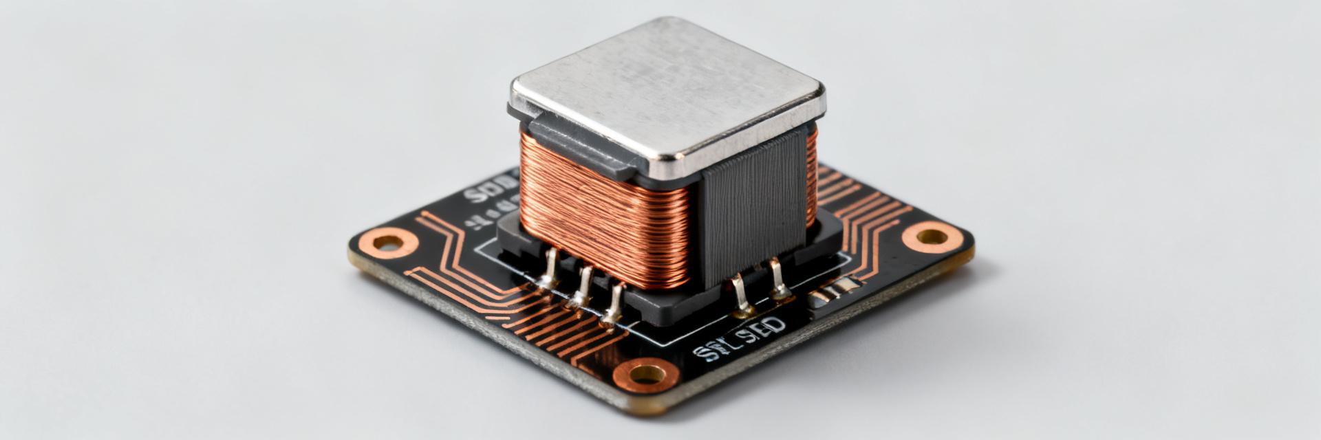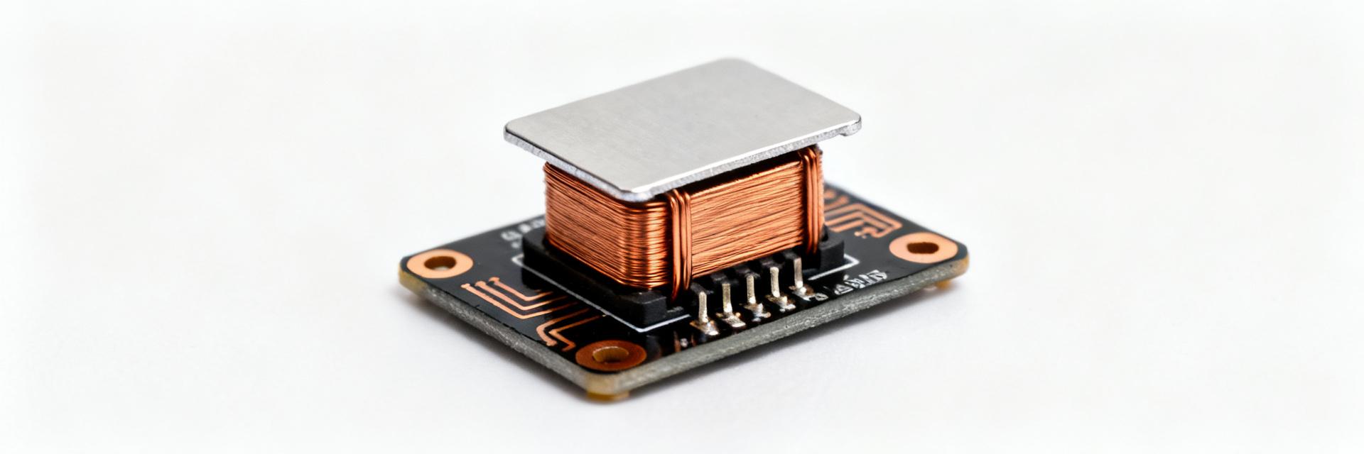
The HPAL1V1265-330-R is documented in the manufacturer datasheet as a 33 µH SMD power inductor with a rated saturation current near 8.0 A under standardized test conditions (100 kHz, 0.1 Vrms, +25°C). For power-design engineers, those headline numbers determine suitability for buck converters, post-regulator LC filters, or hold‑up loops and set expectations for PCB layout, thermal margin, and test validation.
This article uses datasheet baseline numbers to explain key electrical, mechanical, and thermal specs, propose bench tests, and give integration guidance for US power systems. It emphasizes practical measurement steps and procurement checks to validate inductor behavior under DC bias and temperature stress.
Background & Product overview (background introduction)

Part summary and context
Nominal inductance: 33 µH; typical Isat ≈ 8.0 A; SMD two‑pad package and a standard operating temperature window suitable for power rails. This category of power inductor is intended for energy storage in DC–DC converters and attenuation in LC filters, where core material and DCR determine ripple, loss, and thermal rise.
Key datasheet references and test conditions to watch
The datasheet lists test frequency (100 kHz), test voltage (0.1 Vrms) and ambient temperature (+25°C) as measurement baselines. These conditions control open‑circuit inductance (OCL) readings and bias curves; always read footnotes for how Isat or core saturation is reported and whether inductance is measured with or without DC bias.
Key electrical specifications — what they mean for design (data analysis)
Inductance, tolerance, and measurement points
The nominal 33 µH value applies at the datasheet test frequency and no DC bias; tolerance class dictates acceptable variance. When the switching frequency is significantly different from the datasheet test frequency, impedance at that frequency and the effective inductance change. Reference the HPAL1V1265-330-R inductance spec when planning ripple calculations and consider derating if your DC bias or switching frequency reduces effective L below target ripple limits.
Current ratings, saturation (Isat) and current handling (Irms/Dc)
Isat defines the DC current where inductance falls a specified amount (commonly 25%). Irms (or thermal current) relates to heating and copper loss via DCR. Expect DCR to determine I²R losses and temperature rise; use datasheet Isat and DCR to estimate inductance under bias and calculate core plus copper losses for steady‑state and transient conditions.
Mechanical, thermal & environmental specs (data analysis)
Package, PCB mounting, and footprint considerations
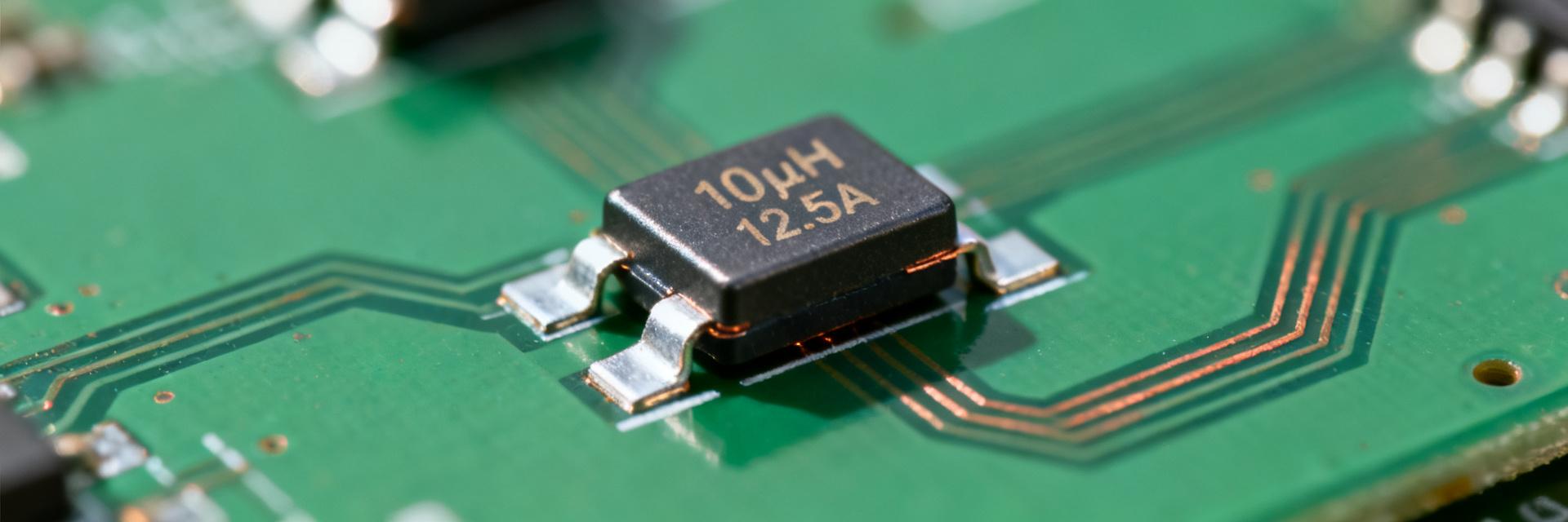
Package is an SMD two‑pad component; recommended land pattern and mechanical drawing on the datasheet should be followed precisely. For thermal relief and current handling, use solid copper pours, thermal vias beneath the copper pour tied to ground or power planes as appropriate, and keep the part clear of high‑heat components to reduce thermal coupling.
Temperature limits, soldering profile and reliability
Observe operating and storage temperature ranges and peak solder reflow temperature limits from the datasheet. DCR typically increases with temperature and inductance can shift; specify margin for expected ambient and hotspot temperatures and choose a solder profile that guarantees mechanical reliability without exceeding the inductor’s peak temperature rating.
Performance tests & real-world measurement plan (method / tests)
Recommended bench tests to validate datasheet claims
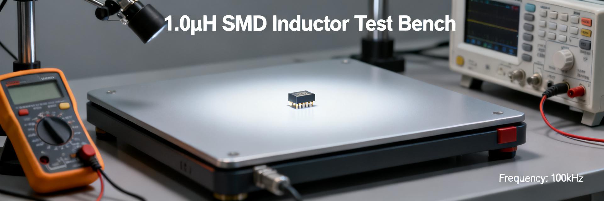
Essential tests: OCL at 100 kHz and 0.1 Vrms, inductance vs DC bias curve, DCR at +25°C, temperature sweep of DCR, ISAT determination (25% inductance drop), and impedance vs frequency. Use an LCR meter with defined test voltage and frequency, a stable current source for bias points, and an oscilloscope for capture of switching node waveforms to assess ripple and saturation symptoms.
Interpreting test results and red flags
Plot L vs DC bias and DCR vs temperature and compare against datasheet tolerances. Red flags include excessive inductance sag at modest bias, DCR higher than spec, audible noise or temperature rise beyond calculated loss. Troubleshoot via reflow profile check, land pattern verification, and repeat sample testing across multiple lots.
Integration & selection guide for common power designs (method / practical)
Choosing HPAL1V1265-330-R for buck converters, filters, and hold-up loops
Match inductance to converter ripple targets: compute ripple current ΔI = Vout*(1−D)/(L*fsw). For 20–40% ripple target, choose L so ΔI sits in that band at expected load. Ensure Isat exceeds peak DC plus transient margin and that DCR keeps temperature rise acceptable for continuous Irms.
PCB layout and EMI mitigation tips
Minimize high‑di/dt loop area between switching node, inductor, and diode/FET; place input decoupling close to supply pins; deploy ground fills and return paths under hot nodes. For EMI, consider snubber networks, common‑mode filters, or selecting lower‑DCR parts if conducted emissions persist.
Application examples, procurement checklist & compliance (case + action)
Short case examples (2 brief scenarios)
Scenario A — 5 V buck at 3 A: a 33 µH device with ~8 A Isat can supply transient peaks; expect reduced inductance under DC bias and model ripple accordingly. Scenario B — post‑regulator LC filter: the part offers substantial attenuation at switching harmonics but require thermal margin and DCR monitoring under continuous load.
Purchasing, inspection & compliance checklist
On receiving parts, verify datasheet items: inductance test conditions, lot‑to‑lot tolerance, recommended land pattern, operating temp and solder profile, and packaging. Perform QC tests: sample inductance vs bias, DCR at +25°C, and visual inspection for mechanical defects. Confirm the datasheet and power inductor parameters match your procurement criteria.
Summary (conclusion)
- HPAL1V1265-330-R is a 33 µH SMD power inductor with ~8.0 A saturation rating; validate inductance versus DC bias to confirm ripple and impedance in your topology.
- Measure DCR and perform a temperature sweep to estimate I²R losses and thermal rise; follow the datasheet land pattern and reflow limits for reliable mounting.
- Run the recommended bench tests (OCL at 100 kHz, L vs DC bias, ISAT, impedance) and apply PCB layout practices to minimize EMI and thermal issues before production.
| Parameter | Value |
|---|---|
| Nominal inductance | 33 µH |
| Typical Isat (25% L drop) | ~8.0 A |
| Irms / DCR (typ) | See datasheet; DCR determines I²R loss |
| Package | SMD, two pads |
| Operating temperature | Refer to datasheet range |
| DC bias (A) | Relative L (% of 33 µH) |
|---|---|
| 0.0 | 100% |
| 2.0 | 92% |
| 4.0 | 78% |
| 6.0 | 60% |
| 8.0 | 42% |
| Temp (°C) | Relative DCR (%) |
|---|---|
| 25 | 100% |
| 50 | 112% |
| 75 | 125% |
| 100 | 140% |
Frequently Asked Questions
What is the expected inductance change under DC bias for this power inductor?
Inductance typically decreases with increasing DC bias; datasheet bias curves show the percent of nominal L at specified currents. Measure L vs DC bias across your expected operating current range to quantify effective inductance and verify it supports your ripple specification.
How should I measure ISAT and interpret the datasheet saturation value?
ISAT is commonly defined as the DC current where L has dropped by a specified percentage (often 25%). Use a stable DC source, measure L at incremental bias currents, and identify the current where the defined L reduction occurs. Treat datasheet Isat as a guideline and add margin for temperature and transients.
Which QC tests are most important on receipt of HPAL1V1265-330-R parts?
Perform batch sample checks: OCL at datasheet conditions, DCR at ambient, and a visual inspection for solderability and mechanical damage. Include a small thermal run to confirm that measured losses and temperature rise align with calculations based on DCR and expected Irms.
What are the best PCB layout practices to mitigate EMI when using the HPAL1V1265-330-R?
Minimize the high-di/dt loop area between the switching node, inductor, and output cap. Keep the switching node trace as short and wide as possible, use solid ground plane return paths directly underneath the component layer, and place input decoupling capacitors close to the power stage supply pins.